Export Gerber Files from KiCad
Exporting Gerber files from KiCad is an essential step to prepare your design for PCB 製造 和 PCB 組裝. These files allow manufacturers to accurately fabricate your board and ensure smooth SMT 組裝 和 交鑰匙 PCB 組裝.
Below is a step-by-step guide to exporting Gerber files from KiCad.
Step 1: Open Your PCB Layout
Open your PCB project in KiCad and launch the PCB Editor (PCBNew).
Before exporting, run a Design Rule Check (DRC) to ensure there are no layout errors that could affect PCB Manufacturing.
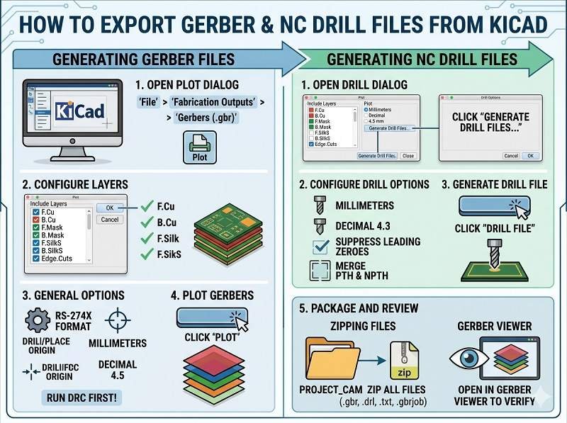
Step 2: Open Plot (Gerber) Settings
In the PCB Editor, go to:
File → Plot
This opens the Gerber export (plot) window where you configure all output settings.
Step 3: Configure General Settings
In the Plot window:
- Set Output format to Gerber
- 選擇 Units (millimeters recommended)
- Set Precision (e.g., 4.6 format)
- Select Use Protel filename extensions (commonly required by manufacturers)
These settings ensure compatibility with standard PCB 製造 流程。.
Step 4: Select Layers to Export
Choose all necessary PCB layers.
Typical layers include:
- F.Cu (Top Copper)
- B.Cu (Bottom Copper)
- Inner layers (for multilayer boards)
- F.Mask (Top Solder Mask)
- B.Mask (Bottom Solder Mask)
- F.SilkS (Top Silkscreen)
- B.SilkS (Bottom Silkscreen)
- Edge.Cuts (Board Outline)
Selecting the correct layers is critical for accurate PCB 組裝.
Step 5: Plot Gerber Files
Click the Plot button to generate Gerber files.
KiCad will export one file per selected layer into your chosen output directory.
Step 6: Generate Drill Files
Gerber files must be accompanied by drill data.
Click Generate Drill Files in the same window.
Configure:
- Drill units (match Gerber units)
- File format (Excellon)
Then click Generate Drill File.
This file defines hole sizes and positions for PCB 製造.
Step 7: Verify Gerber Files
Always verify your Gerber files before sending them for PCB 組裝.
Use KiCad’s built-in Gerber Viewer (GerbView) or a third-party viewer to check:
- Layer alignment
- Board outline accuracy
- Pad and via placement
- Solder mask openings
Verification helps prevent issues during SMT 組裝.
Step 8: Prepare Full Assembly Package
適用於 交鑰匙 PCB 組裝, you should provide a complete set of files:
- Gerber 檔案
- Drill files
- BOM(物料清單)
- Pick and place (centroid) file
- 組裝圖紙
This ensures smooth coordination between PCB fabrication and assembly.
Common Mistakes to Avoid
- Forgetting the Edge.Cuts layer (board outline)
- Missing solder mask or silkscreen layers
- Using inconsistent units between files
- Not generating drill files
- Skipping file verification
Avoiding these mistakes helps ensure a successful PCB Manufacturing process.
總結
Exporting Gerber files from KiCad is a straightforward process when done correctly. By selecting the right layers, generating drill files, and verifying outputs, you can ensure accurate results in PCB 製造, SMT 組裝, 以及 交鑰匙 PCB 組裝.
A complete and correct file package reduces errors, shortens lead times, and guarantees high-quality PCB production.
您的 PCB 裝配解決方案從這裡開始。點選下方索取報價。.
我們提供專業的 PCB 裝配服務,包括 SMT、DIP 及完整的統包解決方案。.
✔ 提供 NDA ✔ 24 小時內快速報價 ✔ ISO 認證工廠 ✔ 一站式 PCB & PCBA 服務


