Export Gerber Files from KiCad
Exporting Gerber files from KiCad is an essential step to prepare your design for PCB Manufacturing and PCB Assembly. These files allow manufacturers to accurately fabricate your board and ensure smooth SMT Assembly and Turnkey PCB Assembly.
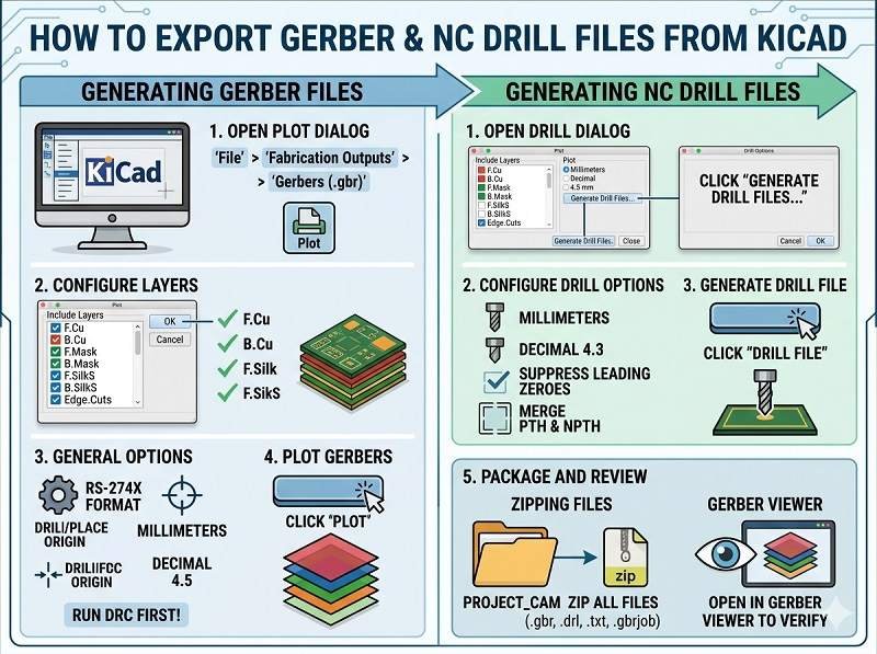
Below is a step-by-step guide to exporting Gerber files from KiCad.
Step 1: Open Your PCB Layout
Open your PCB project in KiCad and launch the PCB Editor (PCBNew).
Before exporting, run a Design Rule Check (DRC) to ensure there are no layout errors that could affect PCB Manufacturing.
Step 2: Open Plot (Gerber) Settings
In the PCB Editor, go to:
File → Plot
This opens the Gerber export (plot) window where you configure all output settings.
Step 3: Configure General Settings
In the Plot window:
- Set Output format to Gerber
- Choose Units (millimeters recommended)
- Set Precision (e.g., 4.6 format)
- Select Use Protel filename extensions (commonly required by manufacturers)
These settings ensure compatibility with standard PCB Manufacturing processes.
Step 4: Select Layers to Export
Choose all necessary PCB layers.
Typical layers include:
- F.Cu (Top Copper)
- B.Cu (Bottom Copper)
- Inner layers (for multilayer boards)
- F.Mask (Top Solder Mask)
- B.Mask (Bottom Solder Mask)
- F.SilkS (Top Silkscreen)
- B.SilkS (Bottom Silkscreen)
- Edge.Cuts (Board Outline)
Selecting the correct layers is critical for accurate PCB Assembly.
Step 5: Plot Gerber Files
Click the Plot button to generate Gerber files.
KiCad will export one file per selected layer into your chosen output directory.
Step 6: Generate Drill Files
Gerber files must be accompanied by drill data.
Click Generate Drill Files in the same window.
Configure:
- Drill units (match Gerber units)
- File format (Excellon)
Then click Generate Drill File.
This file defines hole sizes and positions for PCB Manufacturing.
Step 7: Verify Gerber Files
Always verify your Gerber files before sending them for PCB Assembly.
Use KiCad’s built-in Gerber Viewer (GerbView) or a third-party viewer to check:
- Layer alignment
- Board outline accuracy
- Pad and via placement
- Solder mask openings
Verification helps prevent issues during SMT Assembly.
Step 8: Prepare Full Assembly Package
For Turnkey PCB Assembly, you should provide a complete set of files:
- Gerber files
- Drill files
- BOM (Bill of Materials)
- Pick and place (centroid) file
- Assembly drawings
This ensures smooth coordination between PCB fabrication and assembly.
Common Mistakes to Avoid
- Forgetting the Edge.Cuts layer (board outline)
- Missing solder mask or silkscreen layers
- Using inconsistent units between files
- Not generating drill files
- Skipping file verification
Avoiding these mistakes helps ensure a successful PCB Manufacturing process.
Conclusion
Exporting Gerber files from KiCad is a straightforward process when done correctly. By selecting the right layers, generating drill files, and verifying outputs, you can ensure accurate results in PCB Manufacturing, SMT Assembly, and Turnkey PCB Assembly.
A complete and correct file package reduces errors, shortens lead times, and guarantees high-quality PCB production.
Your PCB assembly solution starts here. Click below to request a quote.
We provide professional PCB assembly services including SMT, DIP, and full turnkey solutions.
✔ NDA Available ✔ Fast Quotation Within 24 Hours ✔ ISO Certified Factory ✔ One-stop PCB & PCBA Service


