PCB Layout Services
Professional PCB Layout Design Services | Optimize for Manufacturability & Performance
Expert PCB Layout Design for Reliable Electronics
A successful electronic product begins with a well-designed PCB layout. It’s the foundation that determines your board’s manufacturability, signal integrity, thermal performance, and long-term reliability. Poor layout choices can lead to costly re-spins, EMI failures, and field failures.
Our professional PCB layout design services bridge the gap between your schematic and a fully manufacturable board. We work as an extension of your engineering team—whether you need a complete layout from scratch, design review, or optimization for cost reduction.

The PCB Layout Design Process
Our structured approach ensures predictability and quality:
Phase 1: Design Review & Stackup Definition
Review schematic and component selection
Define layer stackup (material, thickness, copper weights)
Establish design rules (trace/spacing, via types, clearances
Phase 2: Component Placement
·Logical functional grouping
Thermal and mechanical constraints
Connector and test point accessibility
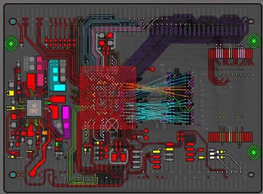
Phase 3: Routing & Optimization
Critical net routing (differential pairs, clocks, sensitive analog)
Power and ground plane design
Design rule checks (DRC) throughout
Phase 4: Design Verification
DFM/DFA review with your fabricator
Signal and power integrity analysis (optional)
Final Gerber generation and documentation package
Phase 5: Handoff & Support
Complete fabrication and assembly package
Ongoing engineering support through prototyping
Why Professional PCB Layout Matters
Many engineers underestimate the impact of layout on production costs and product performance. A professionally designed PCB layout delivers:
| Benefit | Impact on Your Project |
|---|---|
| Manufacturing-Ready Design | DFM/DFA rules applied from day one → fewer revisions, faster time-to-market |
| Controlled Impedance | Proper stackup and trace geometry for high-speed signals (USB, HDMI, DDR, RF) |
| Signal Integrity (SI) | Minimized crosstalk, reflections, and timing issues |
| Power Integrity (PI) | Optimized power distribution network (PDN) with low IR drop and ripple |
| Thermal Management | Strategic component placement and thermal vias for heat dissipation |
| EMI/EMC Compliance | Reduced radiated emissions to pass FCC/CE testing faster |
Expert PCB Layout Design for Reliable Electronics
We handle projects across the full spectrum of complexity:
Board Complexity: Single-layer to 32-layer high-density interconnect (HDI)
Technology: Through-hole, SMT, mixed-technology, rigid-flex
Signal Types: High-speed digital, analog, RF/microwave, power electronics
Design Software: Altium Designer, Allegro, KiCad, PADS (we work with your preferred format)
File Outputs: Gerber (RS-274X), ODB++, IPC-2581, assembly drawings, pick-and-place files

What You Receive
When you engage our PCB layout service, you get a complete, production-ready design package:
Gerber files (with impedance coupons if specified)
NC drill files (through-hole and blind/buried vias)
Assembly drawings (silkscreen, component outlines, polarity markings)
Pick-and-place (centroid) file with X/Y coordinates and rotation
Bill of Materials (BOM) cross-checked against layout
Test point report for in-circuit testing (ICT)
DFM report highlighting any potential manufacturing issues
Industries We Serve
Our layout engineers have experience across:
Industrial controls and automation
Medical devices (ISO 13485 compliant processes)
Automotive electronics (supporting IATF 16949 requirements)
Telecommunications and networking
Consumer electronics
IoT and wireless products


Get Your PCB Layout Project Started
Option 1: Full Layout Service – Send us your schematic and requirements. We deliver complete, manufacturable layout files.
Option 2: Design Review & Optimization – Already have a layout? We’ll review it for DFM, signal integrity, and cost-saving opportunities.
Option 3: Turnkey PCB + Assembly – We take your layout from concept to fully assembled boards, ready for your product.
Need professional PCB layout services for your project?
We provide high-quality PCB design solutions including schematic design, multilayer layout, high-speed routing, and DFM optimization.
Send us your schematics or project requirements and receive a fast, accurate quotation from our experienced engineers.
✔ NDA Available ✔ Fast Quotation Within 24 Hours ✔ Professional Engineering Support