Through-Hole Assembly Process
について through-hole assembly process is a traditional but still widely used method in PCBアセンブリ, where electronic components are inserted into drilled holes on a printed circuit board and then soldered to form strong mechanical and electrical connections. While modern manufacturing relies heavily on SMTアセンブリ, through-hole technology (THT) remains essential for components that require durability, high power handling, or mechanical stability.
Below is a detailed explanation of the through-hole PCB Assembly process.
Overview of Through-Hole Assembly
In through-hole PCB Assembly:
- Component leads are inserted into pre-drilled holes
- Leads pass through the board and are soldered on the opposite side
- Connections are stronger compared to SMT-only designs
This method is commonly used in:
- Power electronics
- 産業機器
- Connectors and transformers
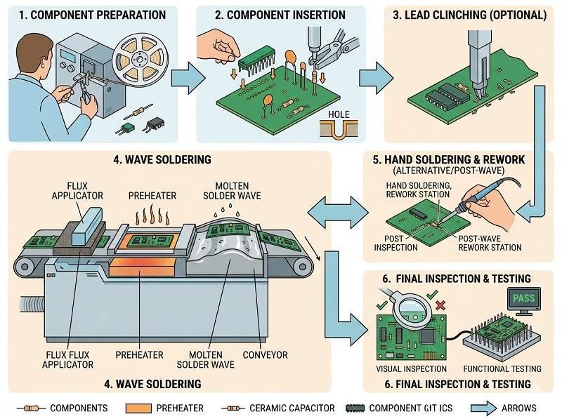
Through-Hole Assembly Process Flow
A standard through-hole PCB Assembly process includes:
- Component preparation
- Component insertion
- Lead trimming
- Soldering (wave or selective)
- 検査と品質管理
- Cleaning and finishing
Each step ensures reliability and structural strength.
Component Preparation
Before assembly begins:
- Components are checked for quality
- Leads may be pre-formed to fit hole spacing
- Parts are organized for efficient insertion
Proper preparation improves assembly efficiency and reduces errors.
Component Insertion
Components are inserted into the PCB:
- Manual insertion: used for low volume or complex boards
- Automated insertion: used in high-volume production
Operators or machines place components into designated holes based on assembly drawings.
リード・トリミング
After insertion:
- Excess leads extending from the bottom of the PCB are trimmed
- Ensures proper soldering and prevents short circuits
This step prepares the board for the soldering process.
Soldering Methods
ウェーブはんだ付け
The most common method in through-hole PCB Assembly:
- The PCB passes over a موجة من solder molten
- Solder attaches to exposed metal leads and pads
- Suitable for high-volume production
選択的はんだ付け
Used for mixed PCBアセンブリ (SMT + through-hole):
- Solder is applied only to specific areas
- Prevents damage to nearby SMT components
Selective soldering offers higher precision.
検査と品質管理
After soldering, inspection ensures quality:
- Visual inspection for solder joints
- AOI(自動光学検査)
- X-ray inspection (if necessary)
Checks include:
- Proper wetting
- No cold joints
- No solder bridges
Cleaning Process
If required:
- Flux residues are removed
- Cleaning improves long-term reliability
This step is important for high-reliability applications.
Final Testing
Through-hole assembled boards may undergo:
- 電気テスト
- 機能テスト
This verifies that the PCB Assembly performs as expected.
Advantages of Through-Hole Assembly
- Strong mechanical bonding
- High reliability in harsh environments
- Suitable for high-power and high-voltage applications
- Better resistance to vibration and thermal stress
Disadvantages Compared to SMT Assembly
- Higher labor cost
- Slower production speed
- Requires drilling holes (higher PCB cost)
- Lower component density
Because of these limitations, through-hole is often combined with SMTアセンブリ in modern designs.
Applications of Through-Hole PCB Assembly
- 産業用制御システム
- カーエレクトロニクス
- 航空宇宙・防衛
- Power supply units
- Large connectors and transformers
Through-Hole vs SMT Assembly
| 特徴 | スルーホールアッセンブリー | SMTアセンブリ |
|---|---|---|
| Mounting method | Leads through holes | Surface mounting |
| Strength | 非常に高い | 中程度 |
| オートメーション | 限定 | Highly automated |
| コスト | より高い | より低い |
| 密度 | より低い | より高い |
結論
The through-hole assembly process remains a critical part of PCBアセンブリ, especially for applications requiring strong mechanical connections and high reliability. Although SMTアセンブリ dominates modern electronics, through-hole technology continues to play an important role in mixed assembly designs.
Understanding both processes allows engineers and buyers to choose the right solution for performance, cost, and durability.
コストと生産の最適化をお手伝いします。今すぐPCBアセンブリのお見積もりをご依頼ください。.
SMT、DIP、フルターンキーソリューションを含むプロフェッショナルなPCBアセンブリサービスを提供します。.
利用できる NDA ✔ 24 時間以内の速い引用語句 ✔ ISO によって証明される工場 ✔ ワンストップ PCB 及び PCBA サービス


