Wave Soldering vs Reflow Soldering in PCB Assembly
Wave soldering and reflow soldering are two widely used soldering methods in PCBアセンブリ. Both processes are essential in PCB製造 そして SMTアセンブリ, but they are designed for different types of components and production requirements.
Understanding the differences between these two methods helps manufacturers choose the right process for efficient and reliable ターンキーPCBアセンブリ.
What is Reflow Soldering
Reflow soldering is primarily used for surface-mount components in SMTアセンブリ.
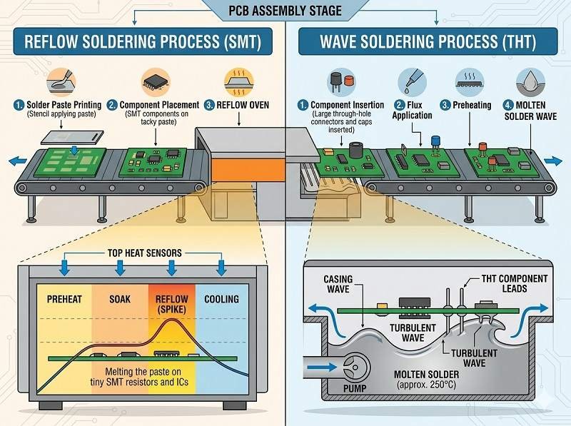
In this process, solder paste is first applied to PCB pads using a stencil. Components are then placed on the board, and the entire assembly is passed through a reflow oven. The heat melts the solder paste, forming strong electrical and mechanical connections.
Key Features of Reflow Soldering
- Ideal for surface-mount devices (SMDs)
- High precision for fine-pitch and small components
- Fully automated and suitable for high-density PCBs
- 現代では一般的 PCBアセンブリ 行
What is Wave Soldering
Wave soldering is mainly used for through-hole components.
In this process, the PCB passes over a موجة (wave) of molten solder. The solder adheres to exposed metal areas, creating connections between component leads and the PCB.
Key Features of Wave Soldering
- Suitable for through-hole components
- Efficient for soldering multiple joints at once
- Commonly used after SMTアセンブリ for mixed-technology boards
- Reliable for strong mechanical connections
Wave Soldering vs Reflow Soldering: Key Differences
Component Type
Reflow soldering is used for surface-mount components in SMTアセンブリ.
Wave soldering is used for through-hole components.
Process Method
Reflow uses controlled heating in an oven to melt solder paste.
Wave soldering uses a موجة of molten solder to form joints.
Automation and Precision
Reflow soldering offers higher precision and is ideal for fine-pitch designs.
Wave soldering is less precise but highly efficient for bulk soldering.
Application in PCB Assembly
Reflow soldering dominates modern PCB製造 due to the widespread use of SMT components.
Wave soldering is still important for connectors, transformers, and other through-hole parts.
When to Use Reflow Soldering
Reflow soldering is best when:
- The design uses surface-mount components
- High-density layouts are required
- Precision and consistency are critical
- Large-scale SMTアセンブリ is involved
When to Use Wave Soldering
Wave soldering is suitable when:
- The PCB includes through-hole components
- Strong mechanical connections are needed
- Mixed-technology boards are used
- Production efficiency is important
Role in Turnkey PCB Assembly
で ターンキーPCBアセンブリ, both methods are often used together.
Reflow soldering handles SMT components.
Wave soldering is used for through-hole components after SMT processes are completed.
This combination ensures efficient and reliable assembly for complex PCB designs.
Advantages and Limitations
Reflow Soldering Advantages
High accuracy and repeatability
Suitable for miniaturized electronics
Compatible with automated SMTアセンブリ
Reflow Soldering Limitations
Not suitable for most through-hole components
Requires precise process control
Wave Soldering Advantages
Efficient for through-hole soldering
Strong and reliable joints
Suitable for batch production
Wave Soldering Limitations
Less suitable for fine-pitch components
Risk of solder bridging if not properly controlled
結論
Wave soldering and reflow soldering are both essential in modern electronics manufacturing. Reflow soldering is the standard for SMTアセンブリ, offering high precision and efficiency, while wave soldering remains important for through-hole components.
で PCBアセンブリ, PCB製造, そして ターンキーPCBアセンブリ, selecting the right soldering method—or combining both—ensures optimal performance, reliability, and production efficiency.
デザインレビューから納品まで、すべてのステップをサポートします。PCBアセンブリのお見積もりをご依頼ください。.
SMT、DIP、フルターンキーソリューションを含むプロフェッショナルなPCBアセンブリサービスを提供します。.
利用できる NDA ✔ 24 時間以内の速い引用語句 ✔ ISO によって証明される工場 ✔ ワンストップ PCB 及び PCBA サービス


