無鉛 PCB 組裝
無鉛印刷電路板組裝是指製造和組裝印刷電路板的過程中不使用鉛 (Pb) 焊接材料。此方法不使用傳統的錫鉛合金,而是使用環保的焊料合金 - 通常由錫、銀和銅(通常稱為 SAC 合金)組成。.
無鉛製程現已成為現代 PCB 組裝 由於 RoHS(有害物質限用)等全球環保法規限制電子產品中有害物質的使用。.
無鉛 PCB 組裝為何重要
採用無鉛 PCB 組裝的主要原因是為了保護環境和健康。鉛是一種有毒物質,如果管理不當,會造成嚴重的健康問題和環境破壞。.
RoHS 等法規已規定許多地區必須進行無鉛製造,尤其是消費性電子產品。因此,大多數 PCB 製造 和 SMT 組裝 目前的製程設計都符合這些標準。.
無鉛與有鉛 PCB 組裝
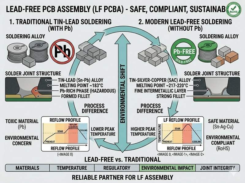
無鉛與傳統有鉛 PCB 組裝的主要差異在於焊料成份。.
有鉛焊料通常使用錫-鉛 (Sn-Pb) 合金,其熔點較低且較易加工。另一方面,無鉛焊料使用的是 SAC305(錫-銀-銅)等合金,其熔點較高,需要更精密的製程控制。.
無鉛焊接通常需要較高的回流焊溫度,這會影響元件選擇和熱能管理。.
無鉛 SMT 組裝製程
無鉛 SMT 組裝 遵循與傳統組裝相似的步驟,但參數有所調整。.
首先,使用鋼版將無鉛焊膏塗在 PCB 上。焊膏中含有 SAC 合金微粒和助焊剂。.
接下來,使用拾取放置機將元件放置到電路板上。.
接著,電路板就會經過回流焊接程序,在此程序中,溫度會比有鉛組裝時更高,以熔化無鉛焊料。.
冷卻後,焊料凝固,形成堅固可靠的接點。.
此製程受到嚴格控制,以確保與元件的相容性,並防止因溫度較高而造成的瑕疵。.
無鉛 PCB 組裝中使用的材料
常見的無鉛焊料合金包括 SAC305(96.5% 錫、3% 銀、0.5% 銅),廣泛應用於電子工業。.
其他材料,例如 PCB 表面處理和元件端子,也必須與無鉛製程相容。這樣才能確保適當的濕潤和可靠的焊點。.
助焊劑配方還針對無鉛焊接進行了優化,以應對更高的溫度並維持性能。.
無鉛 PCB 組裝的挑戰
無鉛 PCB 組裝面臨幾項挑戰。.
較高的回流焊溫度會增加元件和 PCB 的熱應力,可能會影響可靠性。.
如果控制不當,無鉛焊料可能更容易產生某些缺陷,例如空洞或接點變脆。.
製程最佳化至關重要,包括鋼板設計、焊膏選擇和溫度剖析。.
此外,檢查和測試必須確保無鉛接頭符合品質標準。.
交鑰匙 PCB 組裝中的無鉛 PCB 組裝
在 交鑰匙 PCB 組裝, 製造商確保所有材料和製程都符合無鉛標準。這包括 PCB 製造、元件採購、SMT 組裝和最終測試。.
交鑰匙方法簡化了合規性,並確保了整個生產流程的一致性。.
無鉛 PCB 組裝的優勢
無鉛 PCB 組裝具有多項優點。.
它符合國際環保法規,並支持永續製造。.
可降低與鉛接觸相關的健康風險。.
它符合全球市場的要求,允許產品在受監管的地區銷售。.
無鉛 PCB 組裝的應用
幾乎所有現代電子產品都採用無鉛 PCB 組裝。.
應用範圍包括消費性電子產品、汽車系統、醫療設備、工業設備和電信。.
這對於必須符合法規的全球市場產品尤其重要。.
無鉛 PCB 組裝的最佳實踐
為了確保成功,製造商應遵循最佳實務。.
使用高品質的無鉛焊膏和相容材料。.
優化回流焊溫度曲線,防止熱損傷。.
在設計 PCB 時考慮到無鉛製程,包括適當的焊盤設計和表面處理。.
執行嚴格的品質控制與檢驗程序。.
與經驗豐富的 PCB 組裝供應商合作,他們專精於無鉛 SMT 組裝。.
總結
無鉛 PCB 組裝現已成為現代電子製造的產業標準。以環保替代品取代傳統的鉛基焊料,有助於符合法規要求和可持續生產。.
結合先進的 SMT 組裝、PCB 製造和統包 PCB 組裝服務,無鉛製程可確保高品質、可靠且符合全球標準的電子產品。.
您有 PCB 專案嗎?立即索取報價並獲得專家支援。.
我們提供專業的 PCB 裝配服務,包括 SMT、DIP 及完整的統包解決方案。.
✔ 提供 NDA ✔ 24 小時內快速報價 ✔ ISO 認證工廠 ✔ 一站式 PCB & PCBA 服務


