Double-Sided PCB Assembly
Double-sided PCB Assembly refers to the process of mounting electronic components on both sides of a printed circuit board. Unlike single-sided boards, this method utilizes the top and bottom layers of the PCB, allowing for higher component density and more complex circuit designs. It is widely used in modern PCB 組裝 和 SMT 組裝 for compact and high-performance electronic products.
What is a Double-Sided PCB?
A double-sided PCB has:
- Conductive copper layers on both sides
- Through-holes or vias connecting the two sides
- Component placement on both top and bottom surfaces
👉 This structure enables more efficient use of space in PCB 組裝.
Why Use Double-Sided PCB Assembly?
Double-sided assembly offers several advantages:
- 更高的元件密度
- Reduced PCB size
- More complex circuit routing
- Improved functionality in compact designs
👉 It is ideal for modern electronics that require miniaturization.
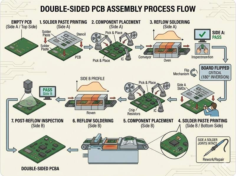
Double-Sided PCB Assembly Process
The process involves assembling components on both sides of the board, typically in stages:
First Side SMT Assembly
- Solder paste printing on the first side
- Component placement using pick-and-place machines
- Reflow soldering to secure components
Second Side SMT Assembly
- PCB is flipped
- Solder paste is applied to the second side
- Components are placed and reflowed again
👉 Adhesives or controlled profiles are used to prevent components from falling during the second reflow.
Through-Hole Component Insertion (Optional)
- Components inserted into plated through-holes
- Followed by wave soldering or selective soldering
Inspection and Testing
- AOI inspection for both sides
- X-ray inspection for hidden joints (if needed)
- Functional testing (FCT)
Key Challenges in Double-Sided Assembly
- Preventing components from dropping during second reflow
- Managing thermal stress from multiple heating cycles
- Ensuring proper alignment on both sides
- Handling heavier components
Techniques to Improve Reliability
- Use of glue dispensing for bottom-side components
- Optimized reflow temperature profiles
- Proper component placement strategy (heavier parts on top side)
- Balanced design to reduce warping
Types of Double-Sided Assembly
SMT on Both Sides
- Most common method
- Uses reflow soldering for both sides
Mixed Assembly
- SMT on one or both sides
- Through-hole components added later
👉 Mixed assembly is common in industrial and power electronics.
Advantages of Double-Sided PCB Assembly
- Maximizes board space
- Reduces overall product size
- Supports complex circuit designs
- Cost-effective compared to multilayer boards (in some cases)
限制條件
- More complex manufacturing process
- Higher assembly cost than single-sided
- Increased risk of defects if not controlled properly
Applications of Double-Sided PCB Assembly
- 消費性電子產品
- 汽車電子
- 工業控制系統
- 通訊裝置
- Medical equipment
Design Considerations
To ensure successful PCB 組裝:
- Place heavier components on the first (top) side
- Ensure adequate spacing between components
- Add fiducials for alignment
- Consider thermal balance during reflow
- Follow DFM and DFA guidelines
Role in PCB Assembly
Double-sided PCB Assembly is a standard approach in modern SMT 組裝, enabling manufacturers to build compact, high-performance electronic devices without significantly increasing board layers.
總結
Double-sided PCB Assembly is a versatile and efficient method in PCB 組裝 和 SMT 組裝, allowing components to be mounted on both sides of a board. While it introduces additional complexity, proper process control and design optimization ensure high reliability and performance in today’s advanced electronics.
準備好開始您的 PCB 裝配專案了嗎?點擊下方快速報價。.
我們提供專業的 PCB 裝配服務,包括 SMT、DIP 及完整的統包解決方案。.
✔ 提供 NDA ✔ 24 小時內快速報價 ✔ ISO 認證工廠 ✔ 一站式 PCB & PCBA 服務


