PCB Rework Process
The PCB rework process refers to the method of correcting defects or replacing components on a printed circuit board after PCBアセンブリ has been completed. It is an essential part of quality control in SMTアセンブリ そして ターンキーPCBアセンブリ, ensuring that defective boards can be repaired instead of scrapped.
Rework is commonly performed when inspection processes identify issues such as solder defects, misaligned components, or faulty parts.
Why PCB Rework Is Necessary
Even with advanced PCB製造 and automated assembly systems, defects can still occur.
Rework allows manufacturers to:
Fix assembly errors without discarding the entire PCB
Reduce production costs
Improve yield rates
Ensure products meet quality standards
It is especially important in high-value or complex SMTアセンブリ プロジェクトに参加している。.
Common Reasons for PCB Rework
Several issues may require rework during or after PCBアセンブリ.
- Solder bridges or shorts
- Insufficient or excessive solder
- Misaligned or misplaced components
- Damaged components
- Incorrect component installation
- Cold solder joints
- BGA or hidden solder joint defects
These problems are often detected through AOI or X-ray inspection.
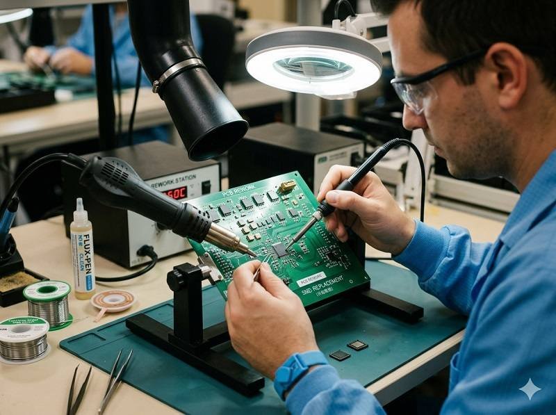
Steps in the PCB Rework Process
The rework process typically involves several controlled steps.
Inspection and Diagnosis
The defect is identified using inspection methods such as AOI, X-ray, or manual inspection.
Component Removal
The faulty component is carefully removed using specialized tools such as hot air rework stations or infrared heaters.
Pad Cleaning
Residual solder is removed from the PCB pads to prepare for reinstallation.
コンポーネント交換
A new component is placed on the PCB with proper alignment.
Resoldering
The component is soldered using controlled heating methods to ensure a reliable connection.
最終検査
The repaired area is inspected again to verify quality and functionality.
Tools Used in PCB Rework
Rework requires specialized equipment to ensure precision and avoid damage.
Hot air rework stations
Infrared (IR) rework systems
Soldering irons with temperature control
Desoldering tools and solder wick
Microscopes for inspection
These tools are essential for handling fine-pitch components in SMTアセンブリ.
Challenges in PCB Rework
Rework can be complex and requires high skill levels.
Excessive heat may damage PCB pads or nearby components.
Repeated rework can weaken solder joints.
Fine-pitch and BGA components are difficult to rework accurately.
Process control is critical to maintain quality in ターンキーPCBアセンブリ.
Best Practices for PCB Rework
信頼できる結果を得るために、メーカーはベストプラクティスに従うべきである。.
Use controlled heating profiles to avoid thermal damage.
Train operators in proper rework techniques.
Minimize the number of rework cycles.
Use high-quality replacement components.
Follow industry standards such as IPC guidelines.
Role in SMT and Turnkey PCB Assembly
で SMTアセンブリ, rework is often used to correct defects identified after reflow soldering.
で ターンキーPCBアセンブリ, it plays a key role in ensuring final product quality before delivery.
Rework helps maintain high yield rates and reduces production waste.
Rework vs Repair
Rework and repair are sometimes confused but are different.
Rework restores a PCB to meet original specifications.
Repair involves fixing a board that may not fully meet original design standards.
Rework is more controlled and standardized in PCB製造.
結論
The PCB rework process is a critical part of modern electronics manufacturing. It enables manufacturers to correct defects, improve yield, and ensure high-quality products without unnecessary waste.
で PCBアセンブリ, SMTアセンブリ, そして ターンキーPCBアセンブリ, effective rework processes help maintain reliability, reduce costs, and deliver consistent performance.
Fast, reliable, and cost-effective PCB assembly solutions. Request your quote now.
SMT、DIP、フルターンキーソリューションを含むプロフェッショナルなPCBアセンブリサービスを提供します。.
利用できる NDA ✔ 24 時間以内の速い引用語句 ✔ ISO によって証明される工場 ✔ ワンストップ PCB 及び PCBA サービス


