奈米 塗層 用於 PCB
用於 PCB 的奈米塗層是一種先進的 保形塗層 它使用奈米技術在電子組件表面形成超薄保護層。它的設計目的是在提供高層次保護的同時,保持最小的厚度,使其成為現代小型化設計的理想選擇。 PCB 組裝 和 SMT 組裝.
什麼是奈米塗層
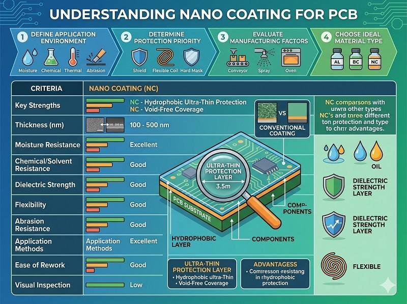
奈米 保形塗層 塗層通常是非常薄的薄膜(通常在納米到微米範圍內),而傳統塗層則要厚得多。儘管它很薄,卻能形成一層非常有效的屏障,阻擋諸如濕氣、灰塵和污染物等環境因素。.
這些塗層通常以先進材料為基礎,例如含氟聚合物或電漿沉積膜,可在分子層級與 PCB 表面結合。.
奈米塗層的主要特性
超薄層
奈米 保形塗層 比傳統塗層薄得多,可在不增加體積或影響高密度元件間距的情況下保護電路。 SMT 組裝.
疏水特性
許多奈米塗層都具有撥水性,可防止濕氣附著在 PCB 表面,降低腐蝕的風險。.
高透明度
塗層通常是透明的,不會干擾檢驗、測試或光學元件。.
對重量和尺寸的影響最小
由於奈米塗層具有極薄的結構,因此非常適合用於小巧輕便的電子裝置。.
優勢 PCB 組裝 和 SMT 組裝
奈米 保形塗層 提供多種優點:
- 出色的防潮和防污染保護
- 保持電氣性能而不改變設計公差
- 適用於緊湊、高密度的 PCB 設計
- 與較厚的塗層相比,允許更容易的返工(在某些情況下)
需要考慮的限制
較低的機械保護
由於厚度較薄,奈米塗層與較厚的塗層 (例如環氧樹脂或聚氨酯) 相比,其物理性與耐磨性較低。.
有限的耐化學性
有些奈米塗層在高侵蝕性的化學環境中可能表現不佳。.
較高的成本和專門製程
等離子鍍膜或氣相鍍膜等應用方法會增加製造複雜性和成本,例如 PCB 組裝.
典型應用
奈米 保形塗層 常用於:
- 消費性電子產品 (智慧型手機、可穿戴式裝置)
- 醫療器材
- 物聯網與精巧型電子模組
- 高密度 SMT 組裝 產品
這些應用可在不影響尺寸或效能的情況下從保護中獲益。.
總結
奈米塗層是一種創新的 保形塗層 以超薄層提供有效的環境保護。在 PCB 組裝 和 SMT 組裝, 對於空間、重量和精確度要求極高的精巧型和高效能電子產品來說,它尤其具有價值。雖然它可能無法在所有情況下取代傳統塗層,但它為下一代電子保護提供了現代化的解決方案。.
取得保形塗層報價
有特殊塗層需求嗎?請將您的 PCB 檔案寄給我們進行評估。.
將您的需求傳送給我們,並獲得我們工程團隊的快速回應。.
24 小時回應 ✔ 工程支援 ✔ 小型與大量生產
深圳市騰欣杰電子有限公司


