DFA Design for Assembly
DFA (Design for Assembly) is a design methodology focused on making products easy, efficient, and cost-effective to assemble. In electronics, DFA ensures that a PCB design is optimized for smooth PCBアセンブリ, especially in automated SMTアセンブリ 環境だ。.
By applying DFA principles, engineers can reduce assembly time, minimize errors, and improve overall production efficiency in both プロトタイプPCBアセンブリ and large-scale manufacturing.
Why DFA is important in PCB Assembly
DFA directly impacts the success of PCBアセンブリ.
Even if a PCB is perfectly manufacturable, poor assembly design can lead to issues such as incorrect component placement, solder defects, or low production yield. DFA helps eliminate these risks by ensuring the design is tailored for real-world assembly conditions.
について プロトタイプPCBアセンブリ, DFA speeds up debugging and iteration. In mass production, it ensures consistent quality and lower costs.
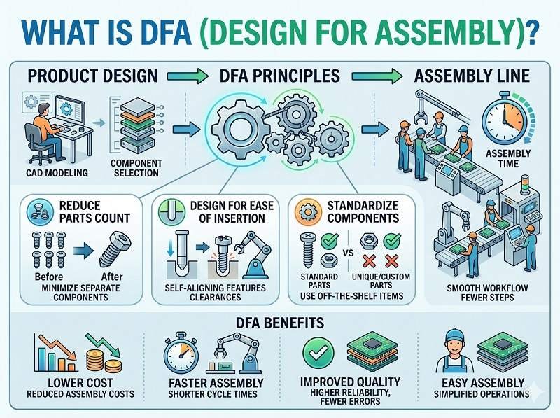
Key principles of DFA in SMT Assembly
DFA focuses on simplifying and optimizing the assembly process.
で SMTアセンブリ, important DFA principles include:
- Using standard component packages whenever possible
- Maintaining consistent component orientation
- Ensuring adequate spacing between components
- Designing clear polarity and reference markings
- Reducing the total number of components
These practices make automated placement easier and reduce the chance of assembly errors.
Component placement optimization
Component placement is one of the most critical aspects of DFA.
Good placement design should:
- Align components in the same direction for machine efficiency
- Group similar components together
- Keep sensitive components away from heat-intensive areas
- Avoid placing components too close to board edges
Optimized placement improves speed and accuracy in PCBアセンブリ and reduces rework.
Soldering and thermal considerations
DFA also addresses soldering quality during SMTアセンブリ.
Designers should consider:
- Balanced pad design to prevent tombstoning
- Proper thermal relief for consistent soldering
- Avoiding shadowing effects in reflow ovens
- Ensuring even heat distribution across the board
These factors are essential for achieving reliable solder joints in PCBアセンブリ.
Common DFA issues
During a DFA review, manufacturers often identify problems such as:
- Components placed too closely together
- Inconsistent orientation of polarized components
- Poor silkscreen labeling
- Difficult-to-access test points
- Mixed technology (SMT and through-hole) without proper planning
Addressing these issues improves assembly efficiency and reduces production risks.
DFA vs DFM
DFA and DFM (Design for Manufacturability) are closely related but focus on different stages.
DFM ensures the PCB can be fabricated correctly during PCB製造, while DFA ensures it can be assembled efficiently during PCBアセンブリ.
Both should be applied together for optimal results in SMTアセンブリ プロジェクトに参加している。.
Benefits of DFA
Applying DFA offers multiple advantages.
It reduces assembly time and labor costs, improves product quality, and minimizes defects. It also enhances automation compatibility, which is critical for modern SMTアセンブリ 線。.
について プロトタイプPCBアセンブリ, DFA reduces troubleshooting time. For mass production, it increases yield and consistency.
When to apply DFA
DFA should be considered during the PCB layout stage, not after the design is complete.
Designers should follow DFA guidelines from the beginning and then perform a review before sending files for PCBアセンブリ そして PCB製造.
Many professional manufacturers also provide DFA feedback as part of their engineering support.
結論
DFA (Design for Assembly) is a key design strategy that ensures your PCB can be assembled efficiently, accurately, and at low cost. By optimizing component placement, orientation, and soldering conditions, DFA improves the overall success of PCBアセンブリ そして SMTアセンブリ.
Whether you are developing a prototype or scaling to mass production, applying DFA principles will help you achieve better quality, faster production, and lower manufacturing costs.
お客様のニーズに合わせたPCBアセンブリのお見積もりをいたします。まずはこちらから.
SMT、DIP、フルターンキーソリューションを含むプロフェッショナルなPCBアセンブリサービスを提供します。.
利用できる NDA ✔ 24 時間以内の速い引用語句 ✔ ISO によって証明される工場 ✔ ワンストップ PCB 及び PCBA サービス


