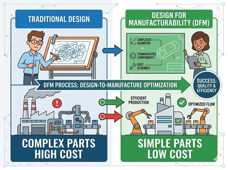
DFM Design for Manufacturability
DFM (Design for Manufacturability) is a design approach that ensures a product can be manufactured efficiently, reliably, and at the lowest possible cost. In the context of electronics, DFM focuses on optimizing PCB designs so they are fully compatible with PCB製造, PCBアセンブリ, そして SMTアセンブリ プロセスがある。.
By applying DFM principles early in the design stage, engineers can prevent production issues, reduce defects, and improve overall product quality.
Why DFM is important in PCB Assembly
DFM plays a critical role in ensuring a smooth transition from design to production.
Without proper DFM, even a functional design may face challenges such as poor solderability, component misalignment, or manufacturing limitations. These issues can lead to delays, increased costs, and failures during PCBアセンブリ.
どちらも プロトタイプPCBアセンブリ and mass production, DFM helps identify potential risks before fabrication begins, saving time and resources.
Key aspects of DFM in PCB Manufacturing
DFM covers multiple areas of PCB design and production.
で PCB製造, DFM ensures that the board can be fabricated within standard process capabilities. This includes:
- Trace width and spacing
- Via size and drill tolerances
- Layer stack-up design
- Solder mask clearance
- Board outline and panelization
Designs that follow DFM guidelines are easier and more cost-effective to produce.
DFM considerations in SMT Assembly
DFM is equally important for SMTアセンブリ, where components are placed and soldered onto the PCB.
Key considerations include:
- Proper pad design for reliable solder joints
- Adequate spacing between components
- Correct component orientation and polarity
- Avoiding shadowing effects during reflow soldering
- Ensuring compatibility with automated placement machines
Good DFM practices improve assembly yield and reduce defects such as tombstoning or solder bridges.
Common DFM issues
Some common problems identified during DFM review include:
- Pads that are too small or improperly shaped
- Components placed too close together
- Inconsistent footprint definitions
- Missing solder mask openings
- Drill holes that are too small for manufacturing capabilities
These issues can negatively impact both PCB製造 そして PCBアセンブリ if not corrected.
DFM vs DFA
DFM is often mentioned together with DFA (Design for Assembly), but they are slightly different.
DFM focuses on how easily a PCB can be fabricated, while DFA focuses on how easily it can be assembled during SMTアセンブリ.
In practice, both are closely related and are usually evaluated together during PCBアセンブリ preparation.
Benefits of applying DFM
Implementing DFM brings several advantages.
It reduces manufacturing costs by optimizing design for standard processes. It improves product quality by minimizing defects. It shortens production time by avoiding redesigns and engineering delays.
について プロトタイプPCBアセンブリ, DFM helps ensure faster iteration cycles. For mass production, it improves yield and consistency.
When to perform DFM
DFM should be applied as early as possible in the design process.
Ideally, designers should follow DFM guidelines during layout and then perform a formal DFM review before sending files for PCB製造 そして PCBアセンブリ.
Many manufacturers also provide DFM checks as part of their service, helping customers refine designs before production.
結論
DFM (Design for Manufacturability) is a critical practice in electronics design that ensures your PCB can be produced efficiently and reliably. By optimizing designs for PCB製造, SMTアセンブリ, そして PCBアセンブリ, DFM reduces costs, improves quality, and minimizes production risks.
あなたが取り組んでいるのは プロトタイプPCBアセンブリ or high-volume production, applying DFM principles is essential for a successful and cost-effective project.
PCBアセンブリのコストを知りたいですか?今すぐ詳細な見積もりをご依頼ください。.
SMT、DIP、フルターンキーソリューションを含むプロフェッショナルなPCBアセンブリサービスを提供します。.
利用できる NDA ✔ 24 時間以内の速い引用語句 ✔ ISO によって証明される工場 ✔ ワンストップ PCB 及び PCBA サービス


