BGA Soldering Process
的 BGA (Ball Grid Array) soldering process is a specialized technique in PCB 組裝 used to mount BGA components onto a printed circuit board. Unlike traditional packages, BGA components have solder balls arranged in a grid underneath the device, making the solder joints hidden from view. This process is widely used in advanced SMT 組裝 due to its ability to support high-density and high-performance electronic designs.
What is a BGA Component?
A BGA package consists of:
- An integrated circuit (IC)
- An array of solder balls on the bottom surface
- A substrate that connects the chip to the solder balls
👉 These solder balls act as both electrical connections and mechanical support during PCB 組裝.
Why BGA is Used in SMT Assembly
BGA components offer several advantages:
- Higher pin density compared to traditional packages
- Better electrical performance (shorter signal paths)
- Improved heat dissipation
- Reduced board space
👉 This makes BGA ideal for modern electronics like smartphones, computers, and industrial devices.
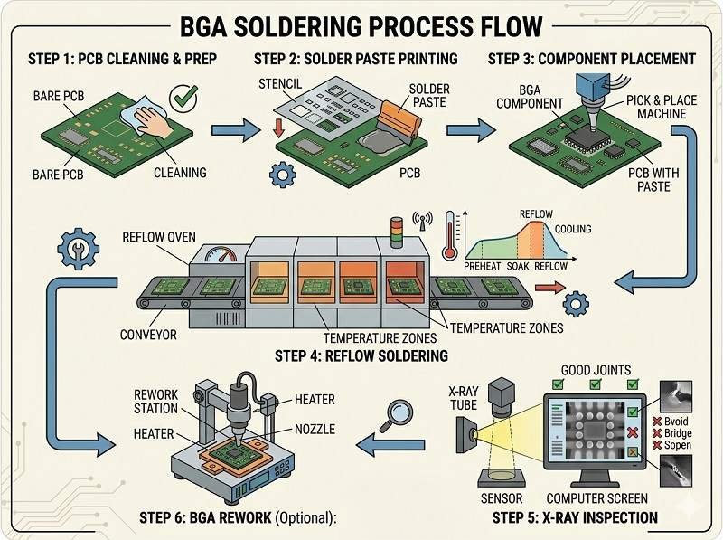
BGA Soldering Process Steps
焊膏印刷
- Solder paste is applied to PCB pads using a stencil
- Accurate volume control is critical
元件安置
- BGA is placed using high-precision pick-and-place machines
- Alignment is crucial since joints are hidden
回流焊接
- The PCB passes through a reflow oven
- Heat melts the solder balls and paste
- Surface tension helps self-align the component
👉 Proper temperature control is essential in SMT 組裝.
冷卻
- Controlled cooling solidifies solder joints
- Prevents defects like cracks or warping
檢查
- X-ray inspection is used to check hidden solder joints
- Ensures connection quality and detects defects
Reflow Profile for BGA
A typical BGA reflow profile includes:
- Preheat stage – Gradual temperature rise
- Soak stage – Activates flux and stabilizes temperature
- Reflow stage – Solder melts (typically 217–245°C for lead-free)
- Cooling stage – Controlled solidification
👉 Optimizing the profile is critical for reliable PCB 組裝.
Common BGA Soldering Defects
BGA soldering can produce defects such as:
- Voids in solder joints
- Head-in-pillow defects
- Bridging between balls
- Open connections
- Misalignment
👉 These defects are difficult to detect without X-ray inspection.
Challenges in BGA Soldering
- Hidden solder joints
- Tight process control requirements
- Sensitivity to temperature and moisture
- Difficulty in rework and repair
BGA Rework Process
If defects occur, BGA components can be reworked:
- Remove the faulty component using controlled heating
- Clean residual solder from pads
- Reball the component (if needed)
- Replace and reflow the component
👉 Rework requires specialized equipment and expertise.
Advantages of BGA Soldering
- Supports high-density PCB designs
- Reliable electrical connections
- Better thermal performance
- Compact and efficient layout
Limitations of BGA Soldering
- Requires advanced inspection (X-ray)
- Higher manufacturing complexity
- Difficult rework process
- Strict process control needed
Applications of BGA in PCB Assembly
BGA soldering is widely used in:
- Consumer electronics (smartphones, laptops)
- 汽車系統
- 工業控制板
- 電信設備
Best Practices for BGA Soldering
- Optimize stencil design and solder paste volume
- Use accurate pick-and-place alignment
- Develop proper reflow temperature profiles
- Control moisture sensitivity (MSL handling)
- Use X-ray inspection for quality assurance
Role in PCB Assembly
在現代 PCB 組裝 和 SMT 組裝, BGA soldering is essential for achieving compact, high-performance designs. It represents a key capability for advanced electronics manufacturing.
總結
The BGA soldering process is a fundamental part of advanced PCB 組裝, enabling high-density and high-performance electronic designs. With precise control over placement, reflow, and inspection, manufacturers can achieve reliable solder joints even in complex SMT 組裝 應用程式。.
您有 PCB 專案嗎?立即索取報價並獲得專家支援。.
我們提供專業的 PCB 裝配服務,包括 SMT、DIP 及完整的統包解決方案。.
✔ 提供 NDA ✔ 24 小時內快速報價 ✔ ISO 認證工廠 ✔ 一站式 PCB & PCBA 服務


