QFN-pakket in PCB-assemblage
Een QFN (Quad Flat No-lead)-pakket is een type opbouwgeïntegreerde schakeling dat wordt gebruikt in PCB-assemblage, gekenmerkt door het ontbreken van uitstekende aansluitdraden. In plaats van pinnen die naar buiten steken, worden de elektrische verbindingen gemaakt via platte metalen pads aan de onderkant van het onderdeel.
QFN-pakketten worden veel gebruikt in moderne SMT-assemblage vanwege hun compacte formaat, uitstekende elektrische prestaties en efficiënte warmteafvoer. Ze worden vaak gebruikt in toepassingen zoals mobiele apparaten, auto-elektronica en communicatiesystemen.
Structuur van een QFN-pakket
Een QFN-pakket bestaat uit een aantal belangrijke elementen.
Aan de onderkant van de verpakking bevinden zich pads die zorgen voor elektrische verbindingen met de printplaat. In het midden is er meestal een groot thermisch pad, dat helpt om de warmte van de chip af te voeren.
Doordat er geen draden nodig zijn, kan de component direct op het PCB-oppervlak zitten, waardoor de inductie afneemt en de signaalintegriteit verbetert. Hierdoor zijn QFN-pakketten ideaal voor toepassingen met hoge frequenties en hoge snelheden.
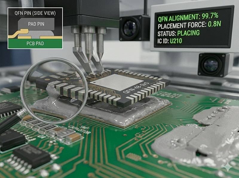
QFN assemblageproces
Het QFN assemblageproces is een nauwkeurig onderdeel van PCB-assemblage en volgt de standaard SMT-procedures met extra overwegingen.
Eerst wordt soldeerpasta aangebracht op de PCB-pads met behulp van een sjabloon. Er wordt speciale aandacht besteed aan het centrale thermische pad, waar het pastapatroon zorgvuldig moet worden gecontroleerd om holtes of te veel soldeer te vermijden.
Vervolgens wordt de QFN-component op de printplaat geplaatst met behulp van uiterst nauwkeurige pick-and-place-machines. Uitlijnen is cruciaal omdat de pads verborgen zitten onder de verpakking.
Vervolgens wordt de printplaat reflow gesoldeerd. Tijdens dit proces smelt de soldeerpasta en vormt verbindingen tussen de QFN-pads en de printplaat.
Na afkoeling stolt het soldeer, waardoor zowel elektrische verbindingen als een thermische verbinding via het blootliggende pad ontstaan.
Uitdagingen in QFN-assemblage
QFN assemblage stelt ons voor verschillende uitdagingen.
Een van de grootste problemen is inspectie. Aangezien de soldeerverbindingen zich onder de component bevinden, zijn ze niet zichtbaar, wat de kwaliteitscontrole complexer maakt.
Thermisch solderen is een andere uitdaging. Een onjuist soldeervolume kan leiden tot holtes, slechte warmteafvoer of zwevende onderdelen.
Nauwkeurige uitlijning is essentieel, want zelfs een kleine verkeerde plaatsing kan leiden tot defecte verbindingen.
Vochtgevoeligheid en hantering vereisen ook zorgvuldige controle om schade tijdens reflow te voorkomen.
Inspectie- en testmethoden
Vanwege de verborgen verbindingen worden gespecialiseerde inspectietechnieken gebruikt.
Röntgeninspectie wordt vaak gebruikt om soldeerverbindingen onder het QFN-pakket te controleren.
Geautomatiseerde optische inspectie (AOI) kan de plaatsing van componenten en de kwaliteit van het soldeer eromheen controleren.
Functioneel testen is ook belangrijk om er zeker van te zijn dat de geassembleerde printplaat correct werkt.
Deze methoden zijn essentieel voor het handhaven van een hoge kwaliteit bij PCB-assemblage met QFN-componenten.
Rol van SMT-assemblage in QFN-verpakking
QFN-pakketten zijn speciaal ontworpen voor SMT-assemblage, die nauwkeurig soldeerpasta printen, nauwkeurige plaatsing en gecontroleerd reflow solderen vereisen.
Geavanceerde SMT assemblageprocessen zorgen ervoor dat QFN componenten betrouwbaar worden gemonteerd, waardoor compacte en krachtige elektronische ontwerpen worden ondersteund.
QFN in Turnkey PCB-assemblage
In Turnkey PCB-assemblage, QFN assemblage wordt uitgevoerd als onderdeel van een complete oplossing die het volgende omvat PCB Productie, Componentsourcing, SMT-assemblage en testen.
Deze geïntegreerde aanpak zorgt ervoor dat het stencilontwerp, de soldeerpastaselectie en reflowprofielen geoptimaliseerd zijn voor QFN-pakketten, waardoor de opbrengst en betrouwbaarheid verbeteren.
Voordelen van QFN-pakketten
QFN-pakketten bieden verschillende voordelen.
Ze nemen weinig ruimte in, waardoor ze ideaal zijn voor compacte apparaten.
Ze bieden uitstekende thermische prestaties dankzij de blootliggende pad.
Ze verbeteren de elektrische prestaties door de parasitaire inductantie te verminderen.
Ze zijn kosteneffectief in vergelijking met complexere verpakkingen.
Toepassingen van QFN-pakketten
QFN-pakketten worden in veel industrieën gebruikt.
Ze worden veel gebruikt in consumentenelektronica, draadloze communicatieapparaten, systemen in auto's en industriële besturingen.
Hun combinatie van compacte afmetingen en hoge prestaties maakt ze geschikt voor moderne PCB-ontwerpen met hoge dichtheid.
Beste praktijken voor QFN-assemblage
Voor een succesvolle QFN assemblage moeten verschillende best practices worden gevolgd.
Ontwerp de PCB-voetafdruk zorgvuldig, inclusief de juiste lay-out van de thermische pad.
Optimaliseer het sjabloonontwerp voor nauwkeurige soldeerpasta-afzetting.
Gebruik de juiste reflowprofielen om goed te solderen.
Implementeer röntgeninspectie voor kwaliteitscontrole.
Werk met ervaren leveranciers van PCB-assemblage die gespecialiseerd zijn in SMT-assemblage en geavanceerde verpakkingstechnologieën.
Conclusie
Een QFN-pakket is een geavanceerd opbouwcomponent dat veel wordt gebruikt in moderne PCB-assemblage. Dankzij het compacte ontwerp, de sterke thermische prestaties en de uitstekende elektrische eigenschappen is het een uitstekende keuze voor toepassingen met hoge dichtheid.
In combinatie met geoptimaliseerde SMT-assemblage, PCB-productie en kant-en-klare PCB-assemblageservices maken QFN-pakketten een betrouwbare en efficiënte productie van hoogwaardige elektronische apparaten mogelijk.
Op zoek naar een betrouwbare PCB assemblage oplossing? Klik hieronder om nu uw offerte aan te vragen.
We bieden professionele assemblagediensten voor printplaten, waaronder SMT, DIP en kant-en-klare oplossingen.
✔ NDA beschikbaar ✔ Snel offerte binnen 24 uur ✔ ISO-gecertificeerde fabriek ✔ One-stop PCB & PCBA Service


