حزمة QFN في تجميع ثنائي الفينيل متعدد الكلور
حزمة QFN (حزمة رباعية مسطحة بدون رصاص) هي نوع من الدوائر المتكاملة ذات التركيب السطحي المستخدمة في تجميع ثنائي الفينيل متعدد الكلور, تتميز بعدم وجود أسلاك بارزة. وبدلاً من المسامير الممتدة للخارج، تتم التوصيلات الكهربائية من خلال وسادات معدنية مسطحة موجودة على الجانب السفلي من المكون.
تُستخدم حزم QFN على نطاق واسع في حزم QFN الحديثة تجميع SMT نظرًا لحجمها الصغير وأدائها الكهربائي الممتاز وكفاءة تبديد الحرارة. وتوجد عادةً في تطبيقات مثل الأجهزة المحمولة وإلكترونيات السيارات وأنظمة الاتصالات.
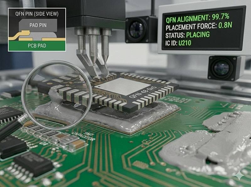
هيكل حزمة QFN
تتكون حزمة QFN من عدة عناصر رئيسية.
في الجزء السفلي من العبوة، توجد وسادات محيطية توفر توصيلات كهربائية بلوحة PCB. وفي الوسط، توجد عادةً وسادة حرارية كبيرة مكشوفة تساعد على تبديد الحرارة من الرقاقة.
يسمح عدم وجود أسلاك توصيل للمكون بالاستقرار مباشرة على سطح ثنائي الفينيل متعدد الكلور، مما يقلل من الحث ويحسن سلامة الإشارة. وهذا يجعل حزم QFN مثالية للتطبيقات عالية التردد وعالية السرعة.
عملية تجميع QFN
تُعد عملية تجميع QFN جزءًا دقيقًا من تجميع ثنائي الفينيل متعدد الكلور ويتبع إجراءات SMT القياسية مع اعتبارات إضافية.
أولاً، يتم وضع معجون اللحام على وسادات ثنائي الفينيل متعدد الكلور باستخدام استنسل. يتم إيلاء اهتمام خاص للوسادة الحرارية المركزية، حيث يجب التحكم في نمط العجينة بعناية لتجنب الفراغات أو اللحام الزائد.
بعد ذلك، يتم وضع مكوّن QFN على ثنائي الفينيل متعدد الكلور باستخدام ماكينات التقاط ووضع عالية الدقة. المحاذاة أمر بالغ الأهمية لأن الوسادات مخفية تحت العبوة.
ثم تخضع اللوحة بعد ذلك لعملية إعادة اللحام. أثناء هذه العملية، يذوب معجون اللحام ويشكل وصلات بين وسادات QFN ولوح ثنائي الفينيل متعدد الكلور.
بعد التبريد، يتصلب اللحام، مما يؤدي إلى إنشاء كل من التوصيلات الكهربائية والترابط الحراري من خلال اللوحة المكشوفة.
التحديات في تجميع QFN
يمثل تجميع QFN العديد من التحديات.
إحدى الصعوبات الرئيسية هي الفحص. نظرًا لأن وصلات اللحام تقع تحت المكون، فهي غير مرئية، مما يجعل التحقق من الجودة أكثر تعقيدًا.
يمثل لحام الوسادة الحرارية تحديًا آخر. يمكن أن يؤدي حجم اللحام غير المناسب إلى حدوث فراغات أو ضعف تبديد الحرارة أو تعويم المكونات.
تُعد دقة المحاذاة أمرًا بالغ الأهمية، حيث يمكن أن يؤدي حتى سوء الوضع الطفيف إلى توصيلات معيبة.
تتطلب حساسية الرطوبة والمناولة أيضًا تحكمًا دقيقًا لمنع التلف أثناء إعادة التدفق.
طرق الفحص والاختبار
نظراً للوصلات المخفية، يتم استخدام تقنيات فحص متخصصة.
يشيع استخدام الفحص بالأشعة السينية لفحص وصلات اللحام أسفل حزمة QFN.
يمكن للفحص البصري الآلي (AOI) التحقق من وضع المكونات وجودة اللحام المحيط بها.
الاختبار الوظيفي مهم أيضاً لضمان أداء اللوحة المجمعة بشكل صحيح.
تعد هذه الطرق ضرورية للحفاظ على الجودة العالية في تجميع ثنائي الفينيل متعدد الكلور الذي يتضمن مكونات QFN.
دور تجميع SMT في التعبئة والتغليف QFN
تم تصميم حزم QFN خصيصًا من أجل تجميع SMT, تتطلب طباعة معجون اللحام بدقة، ووضعه بدقة، والتحكم في إعادة اللحام بإعادة التدفق.
تضمن عمليات تجميع SMT المتقدمة تركيب مكونات QFN بشكل موثوق، مما يدعم التصميمات الإلكترونية المدمجة وعالية الأداء.
QFN في تجميع ثنائي الفينيل متعدد الكلور الجاهز
في تجميع ثنائي الفينيل متعدد الكلور, ، يتم التعامل مع تجميع QFN كجزء من حل متكامل يتضمن تصنيع ثنائي الفينيل متعدد الكلور, وتحديد مصادر المكوّنات، وتجميع SMT، والاختبار.
يضمن هذا النهج المتكامل تحسين تصميم الاستنسل واختيار عجينة اللحام وملامح إعادة التدفق لحزم QFN، مما يحسن الإنتاجية والموثوقية.
مزايا حزم QFN
توفر حزم QFN العديد من المزايا.
فهي توفر بصمة صغيرة، مما يجعلها مثالية للأجهزة المدمجة.
وهي توفر أداءً حرارياً ممتازاً بسبب الوسادة المكشوفة.
فهي تحسن الأداء الكهربائي عن طريق تقليل الحث الطفيلي.
فهي فعالة من حيث التكلفة مقارنةً بأنواع التغليف الأكثر تعقيداً.
تطبيقات حزم QFN
تُستخدم حزم QFN على نطاق واسع في العديد من الصناعات.
وهي شائعة في الإلكترونيات الاستهلاكية، وأجهزة الاتصالات اللاسلكية، وأنظمة السيارات، وأجهزة التحكم الصناعية.
إن الجمع بين الحجم الصغير والأداء العالي يجعلها مناسبة لتصميمات ثنائي الفينيل متعدد الكلور الحديثة عالية الكثافة.
أفضل الممارسات لتجميع QFN
لتحقيق تجميع QFN ناجح، يجب اتباع العديد من أفضل الممارسات.
صمم بصمة ثنائي الفينيل متعدد الكلور بعناية، بما في ذلك تخطيط اللوحة الحرارية المناسبة.
تحسين تصميم الاستنسل من أجل ترسيب دقيق لعجينة اللحام.
استخدم ملفات إعادة التدفق المناسبة لضمان اللحام المناسب.
تنفيذ الفحص بالأشعة السينية لمراقبة الجودة.
اعمل مع مزوّدي تجميع ثنائي الفينيل متعدد الكلور ذوي الخبرة المتخصصين في تجميع SMT وتقنيات التغليف المتقدمة.
الخاتمة
تعد حزمة QFN مكونًا متقدمًا مثبتًا على السطح يستخدم على نطاق واسع في تجميع ثنائي الفينيل متعدد الكلور الحديث. فتصميمها المدمج وأداؤها الحراري القوي وخصائصها الكهربائية الممتازة تجعلها الخيار المفضل للتطبيقات عالية الكثافة.
عند دمجها مع خدمات تجميع SMT المحسّنة، وتصنيع ثنائي الفينيل متعدد الكلور، وخدمات تجميع ثنائي الفينيل متعدد الكلور بنظام تسليم المفتاح، تتيح حزم QFN إنتاجًا موثوقًا وفعالًا للأجهزة الإلكترونية عالية الأداء.
هل تبحث عن حل موثوق لتجميع ثنائي الفينيل متعدد الكلور؟ انقر أدناه لطلب عرض الأسعار الآن.
نحن نوفر خدمات تجميع ثنائي الفينيل متعدد الكلور الاحترافية بما في ذلك SMT وDIP وحلول تسليم المفتاح الكاملة.
✔ إتاحة اتفاقية عدم الإفشاء ✔ عرض أسعار سريع في غضون 24 ساعة ✔ مصنع معتمد من ISO ✔ خدمة PCB و PCBA الشاملة


