PCB 어셈블리의 QFN 패키지
QFN(쿼드 플랫 무연) 패키지는 다음 분야에서 사용되는 표면 실장 집적 회로의 한 유형입니다. PCB 어셈블리, 튀어나온 리드가 없는 것이 특징입니다. 바깥쪽으로 뻗어 있는 핀 대신 구성 요소의 밑면에 있는 평평한 금속 패드를 통해 전기 연결이 이루어집니다.
QFN 패키지는 현대식 SMT 어셈블리 컴팩트한 크기, 뛰어난 전기적 성능, 효율적인 열 방출로 인해 널리 사용되고 있습니다. 모바일 장치, 자동차 전자 장치, 통신 시스템과 같은 애플리케이션에서 흔히 볼 수 있습니다.
QFN 패키지의 구조
QFN 패키지는 몇 가지 주요 요소로 구성됩니다.
패키지 하단에는 PCB에 전기 연결을 제공하는 주변 패드가 있습니다. 중앙에는 일반적으로 칩의 열을 방출하는 데 도움이 되는 커다란 열 패드가 노출되어 있습니다.
리드가 없기 때문에 부품을 PCB 표면에 직접 배치할 수 있어 인덕턴스가 감소하고 신호 무결성이 향상됩니다. 따라서 QFN 패키지는 고주파 및 고속 애플리케이션에 이상적입니다.
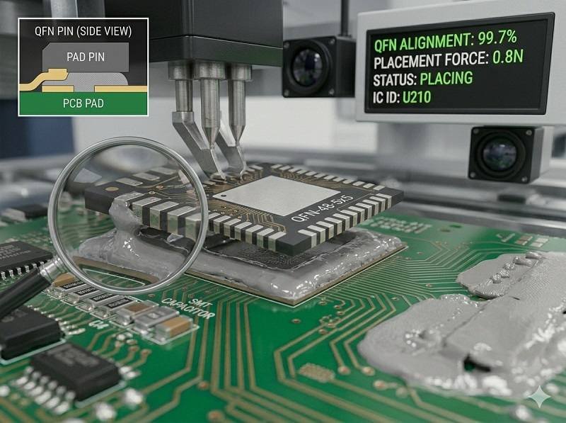
QFN 조립 프로세스
QFN 조립 공정은 다음과 같이 정밀한 부분입니다. PCB 어셈블리 추가 고려 사항이 있는 표준 SMT 절차를 따릅니다.
먼저 스텐실을 사용하여 솔더 페이스트를 PCB 패드에 도포합니다. 공극이나 과도한 납땜을 방지하기 위해 페이스트 패턴을 세심하게 제어해야 하는 중앙 열 패드에 특히 주의를 기울입니다.
다음으로 고정밀 픽 앤 플레이스 머신을 사용하여 QFN 부품을 PCB에 배치합니다. 패드가 패키지 아래에 숨겨져 있기 때문에 정렬이 매우 중요합니다.
그런 다음 기판은 리플로 납땜을 거칩니다. 이 과정에서 솔더 페이스트가 녹아 QFN 패드와 PCB 사이에 연결이 형성됩니다.
냉각 후 땜납이 굳어지면 노출된 패드를 통해 전기 연결과 열 접착이 모두 이루어집니다.
QFN 조립의 과제
QFN 조립에는 몇 가지 어려움이 있습니다.
가장 큰 어려움 중 하나는 검사입니다. 납땜 접합부는 부품 아래에 위치하기 때문에 눈에 보이지 않아 품질 검증이 더 복잡해집니다.
열 패드 납땜은 또 다른 과제입니다. 납땜량이 부적절하면 공극, 열 방출 불량 또는 부품 부유가 발생할 수 있습니다.
조금만 잘못 배치해도 연결에 결함이 생길 수 있으므로 정렬 정확도는 매우 중요합니다.
리플로우 중 손상을 방지하기 위해 습기 민감도와 취급에 대한 세심한 관리도 필요합니다.
검사 및 테스트 방법
숨겨진 조인트 때문에 특수 검사 기법이 사용됩니다.
X-레이 검사는 일반적으로 QFN 패키지 아래의 납땜 접합부를 검사하는 데 사용됩니다.
자동 광학 검사(AOI)는 부품 배치와 주변 납땜 품질을 확인할 수 있습니다.
조립된 보드가 올바르게 작동하는지 확인하기 위해 기능 테스트도 중요합니다.
이러한 방법은 QFN 부품이 포함된 PCB 조립에서 높은 품질을 유지하는 데 필수적입니다.
QFN 패키징에서 SMT 조립의 역할
QFN 패키지는 다음을 위해 특별히 설계되었습니다. SMT 어셈블리, 정밀한 솔더 페이스트 인쇄, 정확한 배치 및 제어된 리플로우 납땜이 필요합니다.
고급 SMT 어셈블리 공정은 QFN 부품을 안정적으로 실장하여 컴팩트한 고성능 전자 설계를 지원합니다.
턴키 PCB 어셈블리의 QFN
In 턴키 PCB 어셈블리, QFN 어셈블리는 다음을 포함하는 전체 솔루션의 일부로 처리됩니다. PCB 제조, 부품 소싱, SMT 조립 및 테스트.
이러한 통합 접근 방식을 통해 스텐실 설계, 솔더 페이스트 선택, 리플로 프로파일이 QFN 패키지에 최적화되어 수율과 신뢰성이 향상됩니다.
QFN 패키지의 장점
QFN 패키지는 여러 가지 이점을 제공합니다.
설치 공간이 작아 소형 디바이스에 이상적입니다.
노출된 패드로 인해 뛰어난 열 성능을 제공합니다.
기생 인덕턴스를 줄여 전기적 성능을 향상시킵니다.
더 복잡한 패키징 유형에 비해 비용 효율적입니다.
QFN 패키지의 응용 분야
QFN 패키지는 여러 산업 분야에서 널리 사용되고 있습니다.
소비자 가전, 무선 통신 장치, 자동차 시스템 및 산업 제어 장치에서 흔히 볼 수 있습니다.
컴팩트한 크기와 고성능의 조합으로 최신 고밀도 PCB 설계에 적합합니다.
QFN 조립 모범 사례
성공적인 QFN 조립을 위해서는 몇 가지 모범 사례를 따라야 합니다.
적절한 써멀 패드 레이아웃을 포함하여 PCB 풋프린트를 신중하게 설계하세요.
정확한 솔더 페이스트 증착을 위해 스텐실 설계를 최적화합니다.
적절한 리플로 프로파일을 사용하여 적절한 납땜을 보장합니다.
품질 관리를 위해 X-레이 검사를 구현합니다.
SMT 어셈블리 및 고급 패키징 기술을 전문으로 하는 숙련된 PCB 어셈블리 제공업체와 협력하세요.
결론
QFN 패키지는 최신 PCB 조립에 널리 사용되는 고급 표면 실장 부품입니다. 컴팩트한 디자인, 강력한 열 성능, 뛰어난 전기적 특성으로 고밀도 애플리케이션에 선호되는 부품입니다.
최적화된 SMT 조립, PCB 제조 및 턴키 PCB 조립 서비스와 결합하면 QFN 패키지를 통해 고성능 전자 장치를 안정적이고 효율적으로 생산할 수 있습니다.
신뢰할 수 있는 PCB 어셈블리 솔루션을 찾고 계신가요? 지금 견적을 요청하려면 아래를 클릭하세요.
당사는 SMT, DIP 및 전체 턴키 솔루션을 포함한 전문 PCB 조립 서비스를 제공합니다.
NDA 가능 ✔ 24시간 이내 빠른 견적 ✔ ISO 인증 공장 ✔ 원스톱 PCB 및 PCBA 서비스


