
BGA solder inspection in modern PCB manufacturing
Ball Grid Array (BGA) components are widely used in modern electronics because they allow high-density connections and better electrical performance in compact designs. However, inspecting BGA solder joints is much more complex than traditional components because the solder joints are hidden underneath the package.
현대 PCB 어셈블리, especially in high-density products, BGA inspection has become a critical part of quality control. The same applies to 프로토타입 PCB 어셈블리, where early-stage testing helps identify process or design issues before mass production. In large-scale PCB 제조, consistent inspection ensures product stability and long-term reliability.
Why BGA solder joint inspection is critical
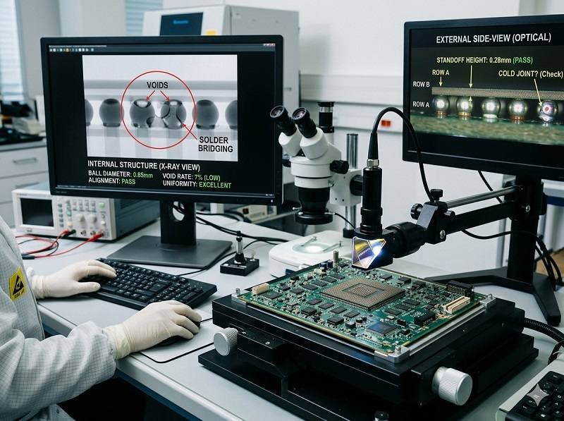
The biggest issue with BGA components is that defects are not visible from the outside. Unlike traditional solder joints, BGA connections cannot be checked with simple visual inspection after reflow.
Common problems include voids inside solder balls, cold solder joints, bridging, misalignment, and head-in-pillow defects. These issues may not appear immediately but can lead to serious failures during operation.
This is why in SMT 어셈블리, BGA inspection is considered a mandatory quality control step rather than an optional process.
Challenges in inspecting BGA solder joints
The main challenge is obvious: the solder joints are completely hidden under the component. This makes traditional optical inspection ineffective.
현대 PCB 제조, additional challenges include miniaturization of components, high-density layouts, lead-free solder behavior, and multilayer PCB structures. All of these factors make BGA inspection more complex and require advanced detection methods instead of simple visual checks.
X-ray inspection for BGA solder joints
X-ray inspection is the most widely used and reliable method for BGA analysis in PCB 어셈블리.
2D X-ray inspection
2D X-ray provides a flat image of the solder joints and is commonly used on production lines. It is effective for detecting voids, missing solder balls, bridging issues, and general alignment problems.
In SMT 어셈블리, this method is widely used because it is fast and suitable for high-volume inspection.
3D X-ray (CT inspection)
3D X-ray, also known as CT scanning, provides a more detailed internal view of the solder structure. It is widely used in high-reliability PCB 제조 환경으로 이동합니다.
This method can detect more advanced defects such as head-in-pillow, internal cracks, and uneven void distribution. In 프로토타입 PCB 어셈블리, it is especially useful for validating new designs and improving process parameters.
AOI in SMT assembly and its limitations
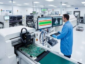
Automated Optical Inspection (AOI) is a standard process in most SMT 어셈블리 lines. It plays an important role in detecting placement and surface-level issues.
AOI can check component alignment, missing parts, polarity issues, and solder paste quality before reflow. However, it cannot inspect the actual BGA solder joints because they are hidden under the package.
Therefore, in PCB 어셈블리, AOI is always combined with X-ray inspection to achieve complete coverage.
Microsection analysis for failure investigation
When deeper analysis is required, microsectioning is used. This is a destructive method where the PCB is physically cut to examine solder joints under a microscope.
In PCB 제조, this method is used for failure analysis, root cause investigation, and studying solder joint structure. It is especially valuable in 프로토타입 PCB 어셈블리, where engineers need detailed feedback during development.
Electrical testing for BGA reliability
Inspection alone is not enough. Electrical testing is also required to ensure the board works correctly in real conditions.
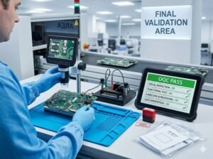
In PCB 어셈블리, common testing methods include in-circuit testing (ICT), functional testing (FCT), burn-in testing, and thermal cycling tests. These methods help detect hidden electrical failures that cannot be seen through imaging alone.
Common BGA defects and how they are detected
Different inspection methods are used depending on the type of defect.
Voids are typically detected using X-ray inspection. Bridging issues can be identified through both X-ray and AOI. Head-in-pillow defects require 3D X-ray analysis. Cold solder joints are usually found through functional testing. Misalignment issues can be detected early by AOI before reflow.
By combining multiple methods, SMT 어셈블리 processes can significantly improve product reliability.
Process control to prevent BGA defects
Good inspection is important, but preventing defects in the first place is even more critical.
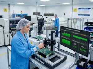
In PCB 제조, manufacturers focus on process optimization such as solder paste printing accuracy, reflow temperature control, PCB pad design, component storage conditions, and clean production environments.
In 프로토타입 PCB 어셈블리, these parameters are often adjusted repeatedly to achieve stable production results before scaling up.
결론
BGA solder joint inspection is a key part of modern electronics manufacturing. Since defects are hidden, manufacturers must rely on a combination of X-ray inspection, AOI support, electrical testing, and process optimization.
In PCB 어셈블리, 프로토타입 PCB 어셈블리, SMT 어셈블리, 및 PCB 제조, a well-designed inspection strategy ensures higher product quality, lower failure rates, and improved long-term reliability.
PCB 프로젝트를 염두에 두고 계신가요? 지금 바로 견적을 요청하고 전문가의 지원을 받으세요.
당사는 SMT, DIP 및 전체 턴키 솔루션을 포함한 전문 PCB 조립 서비스를 제공합니다.
NDA 가능 ✔ 24시간 이내 빠른 견적 ✔ ISO 인증 공장 ✔ 원스톱 PCB 및 PCBA 서비스
 한국어
한국어  English
  Deutsch
  Français
  Português do Brasil
  Español
  日本語
日本語  Nederlands
  Italiano
  Русский
  العربية
  Svenska
  Polski
  Türkçe
  繁體中文
繁體中文