Multilayer PCB Assembly
Multilayer PCB Assembly refers to the process of assembling electronic components onto a printed circuit board that contains three or more conductive layers. Unlike single-sided or double-sided boards, multilayer PCBs stack multiple copper layers separated by insulating materials, enabling highly complex and compact circuit designs. This type of assembly is widely used in advanced Montaż PCB oraz Montaż SMT for high-performance electronic products.
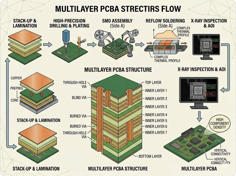
What is a Multilayer PCB?
A multilayer PCB typically includes:
- Multiple copper layers (4, 6, 8, or more)
- Insulating layers (prepreg and core materials)
- Vias (through-hole, blind, and buried vias)
- Internal routing for signals, power, and ground
👉 These layers are laminated together to form a single compact board used in modern Montaż PCB.
Why Use Multilayer PCB Assembly?
Multilayer designs are essential for:
- High-density circuits
- Complex signal routing
- High-speed and high-frequency applications
- Miniaturized electronic devices
👉 They allow more functionality in a smaller footprint compared to traditional PCBs.
Multilayer PCB Assembly Process
The assembly process is similar to standard Montaż SMT, but with tighter control requirements:
Drukowanie pasty lutowniczej
- Precise application on surface pads
- Critical for fine-pitch components
Rozmieszczenie komponentów
- High-speed, high-accuracy pick-and-place machines
- Handles dense layouts and small components
Lutowanie rozpływowe
- Controlled temperature profile
- Ensures reliable solder joints without damaging inner layers
Kontrola
- AOI for surface defects
- X-ray inspection for hidden joints and internal connections
Testowanie
- ICT (In-Circuit Testing) for electrical validation
- Functional testing (FCT) for system performance
Key Features of Multilayer PCB Assembly
- High component density
- Complex routing capability
- Improved signal integrity
- Reduced electromagnetic interference (EMI)
👉 These features make multilayer boards essential in advanced electronics.
Challenges in Multilayer PCB Assembly
- More complex design and manufacturing
- Higher cost compared to simpler PCBs
- Difficult inspection of internal layers
- Thermal management issues
- Increased risk of defects if not properly controlled
Advantages of Multilayer PCB Assembly
- Compact and lightweight design
- High reliability and durability
- Better electrical performance
- Supports high-speed signal transmission
- Reduced noise and interference
Applications of Multilayer PCB Assembly
Multilayer PCB Assembly is widely used in:
- Smartphones and consumer electronics
- Computers and servers
- Elektronika samochodowa
- Systemy lotnicze i kosmiczne
- Urządzenia medyczne
- Sprzęt telekomunikacyjny
Design Considerations
To ensure successful Montaż PCB:
- Optimize layer stack-up design
- Control impedance for high-speed signals
- Ensure proper via design (blind/buried vias)
- Plan thermal management (heat dissipation)
- Follow DFM, DFA, and DFT guidelines
Multilayer vs Double-Sided PCB Assembly
| Cecha | Multilayer PCB | Double-Sided PCB |
|---|---|---|
| Warstwy | 3 or more | 2 |
| Złożoność | Wysoki | Umiarkowany |
| Koszt | Wyższy | Niższy |
| Wydajność | Zaawansowany | Basic to moderate |
👉 Multilayer PCBs are used when higher performance and density are required.
Role in Modern SMT Assembly
In today’s Montaż SMT, multilayer PCB Assembly is essential for:
- Miniaturized devices
- High-speed communication systems
- Advanced computing hardware
It represents the standard for modern electronics manufacturing.
Wnioski
Multilayer PCB Assembly is a key technology in advanced Montaż PCB oraz Montaż SMT, enabling complex, high-performance, and compact electronic designs. While it involves higher cost and complexity, its benefits in performance, reliability, and miniaturization make it indispensable in modern electronic products.
Chcesz poznać koszt montażu PCB? Poproś o szczegółową wycenę już teraz.
Zapewniamy profesjonalne usługi montażu PCB, w tym SMT, DIP i pełne rozwiązania "pod klucz".
✔ Dostępna NDA ✔ Szybka wycena w ciągu 24 godzin ✔ Fabryka z certyfikatem ISO ✔ Kompleksowy serwis PCB i PCBA


