Multilayer PCB Assembly
Multilayer PCB Assembly refers to the process of assembling electronic components onto a printed circuit board that contains three or more conductive layers. Unlike single-sided or double-sided boards, multilayer PCBs stack multiple copper layers separated by insulating materials, enabling highly complex and compact circuit designs. This type of assembly is widely used in advanced PCB-assemblage en SMT-assemblage for high-performance electronic products.
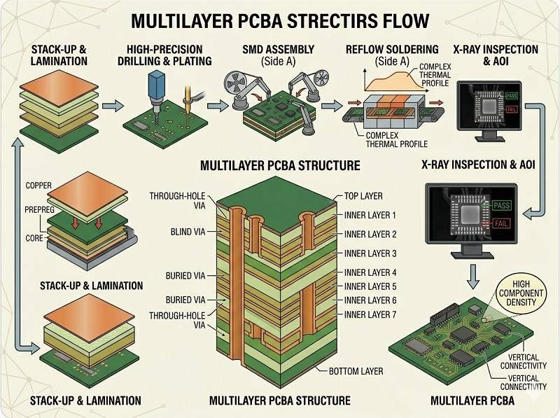
What is a Multilayer PCB?
A multilayer PCB typically includes:
- Multiple copper layers (4, 6, 8, or more)
- Insulating layers (prepreg and core materials)
- Vias (through-hole, blind, and buried vias)
- Internal routing for signals, power, and ground
👉 These layers are laminated together to form a single compact board used in modern PCB-assemblage.
Why Use Multilayer PCB Assembly?
Multilayer designs are essential for:
- High-density circuits
- Complex signal routing
- High-speed and high-frequency applications
- Miniaturized electronic devices
👉 They allow more functionality in a smaller footprint compared to traditional PCBs.
Multilayer PCB Assembly Process
The assembly process is similar to standard SMT-assemblage, but with tighter control requirements:
Soldeerpasta afdrukken
- Precise application on surface pads
- Critical for fine-pitch components
Plaatsing van onderdelen
- High-speed, high-accuracy pick-and-place machines
- Handles dense layouts and small components
Reflow-solderen
- Controlled temperature profile
- Ensures reliable solder joints without damaging inner layers
Inspectie
- AOI for surface defects
- X-ray inspection for hidden joints and internal connections
Testen
- ICT (In-Circuit Testing) for electrical validation
- Functional testing (FCT) for system performance
Key Features of Multilayer PCB Assembly
- High component density
- Complex routing capability
- Improved signal integrity
- Reduced electromagnetic interference (EMI)
👉 These features make multilayer boards essential in advanced electronics.
Challenges in Multilayer PCB Assembly
- More complex design and manufacturing
- Higher cost compared to simpler PCBs
- Difficult inspection of internal layers
- Thermal management issues
- Increased risk of defects if not properly controlled
Advantages of Multilayer PCB Assembly
- Compact and lightweight design
- High reliability and durability
- Better electrical performance
- Supports high-speed signal transmission
- Reduced noise and interference
Applications of Multilayer PCB Assembly
Multilayer PCB Assembly is widely used in:
- Smartphones and consumer electronics
- Computers and servers
- Automobielelektronica
- Ruimtevaartsystemen
- Medische apparaten
- Telecommunicatieapparatuur
Design Considerations
To ensure successful PCB-assemblage:
- Optimize layer stack-up design
- Control impedance for high-speed signals
- Ensure proper via design (blind/buried vias)
- Plan thermal management (heat dissipation)
- Follow DFM, DFA, and DFT guidelines
Multilayer vs Double-Sided PCB Assembly
| Functie | Multilayer PCB | Double-Sided PCB |
|---|---|---|
| Lagen | 3 or more | 2 |
| Complexiteit | Hoog | Matig |
| Kosten | Hoger | Onder |
| Prestaties | Geavanceerd | Basic to moderate |
👉 Multilayer PCBs are used when higher performance and density are required.
Role in Modern SMT Assembly
In today’s SMT-assemblage, multilayer PCB Assembly is essential for:
- Miniaturized devices
- High-speed communication systems
- Advanced computing hardware
It represents the standard for modern electronics manufacturing.
Conclusie
Multilayer PCB Assembly is a key technology in advanced PCB-assemblage en SMT-assemblage, enabling complex, high-performance, and compact electronic designs. While it involves higher cost and complexity, its benefits in performance, reliability, and miniaturization make it indispensable in modern electronic products.
Wilt u de kosten van uw PCB assemblage weten? Vraag dan nu een gedetailleerde offerte aan.
We bieden professionele assemblagediensten voor printplaten, waaronder SMT, DIP en kant-en-klare oplossingen.
✔ NDA beschikbaar ✔ Snel offerte binnen 24 uur ✔ ISO-gecertificeerde fabriek ✔ One-stop PCB & PCBA Service


