DFT Design for Testing
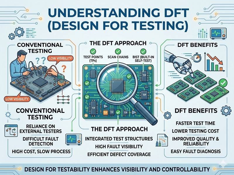
DFT (Design for Testing) is a design methodology that ensures a product can be easily and effectively tested during and after manufacturing. In electronics, DFT focuses on designing PCBs so they can be inspected, verified, and debugged efficiently throughout تجميع ثنائي الفينيل متعدد الكلور, تجميع SMT, و تصنيع ثنائي الفينيل متعدد الكلور العمليات.
By integrating testing considerations early in the design stage, DFT helps improve product quality, reduce defects, and lower long-term production costs.
Why DFT is important in PCB Assembly
DFT plays a critical role in ensuring product reliability.
Without proper test access and planning, it becomes difficult to detect faults such as open circuits, short circuits, or incorrect component placement during تجميع ثنائي الفينيل متعدد الكلور. This can lead to defective products reaching customers or increased rework costs.
لكل من تجميع النموذج الأولي لثنائي الفينيل متعدد الكلور and mass production, DFT ensures that every board can be tested quickly and accurately.
Key objectives of DFT
The main goal of DFT is to make testing easier, faster, and more reliable.
في تجميع SMT, this includes:
- Providing access to critical electrical nodes
- Enabling automated test equipment (ATE) compatibility
- Reducing test time and complexity
- Improving fault detection and diagnosis
A well-designed DFT strategy ensures efficient validation during تجميع ثنائي الفينيل متعدد الكلور.
Common testing methods supported by DFT
DFT enables several types of testing used in تصنيع ثنائي الفينيل متعدد الكلور and assembly.
These include:
- In-Circuit Testing (ICT): checks individual components and connections
- Functional Testing (FCT): verifies the board operates as intended
- Flying Probe Testing: used for تجميع النموذج الأولي لثنائي الفينيل متعدد الكلور without fixtures
- Boundary Scan (JTAG): tests complex ICs and interconnections
Each method requires specific design considerations, which DFT helps address.
Test point design and placement
Test points are essential in DFT.
Designers should include accessible test pads for key signals, power lines, and ground. These test points allow probes or fixtures to connect easily during تجميع ثنائي الفينيل متعدد الكلور testing.
Best practices include:
- Sufficient spacing between test points
- Consistent test pad size
- Clear labeling and documentation
- Avoiding placement under components
Proper test point design ensures reliable testing in تجميع SMT البيئات.
Design considerations for DFT
Several factors should be considered to implement effective DFT.
These include:
- Ensuring good access to critical signals
- Avoiding densely packed areas that block probes
- Designing stable power distribution for testing
- Including debugging interfaces (e.g., UART, JTAG)
- Planning for test fixtures early
These considerations improve test coverage and reduce troubleshooting time.
Common DFT issues
Without proper DFT, manufacturers may encounter problems such as:
- Limited access to test points
- Incomplete test coverage
- Difficulty diagnosing failures
- Increased testing time and cost
These issues can significantly impact efficiency in both تجميع ثنائي الفينيل متعدد الكلور و تجميع SMT.
Benefits of DFT
Applying DFT provides several advantages.
It improves product quality by detecting defects early, reduces rework costs, and speeds up production testing. It also enhances reliability, which is especially important for complex or high-reliability electronics.
بالنسبة لـ تجميع النموذج الأولي لثنائي الفينيل متعدد الكلور, DFT simplifies debugging. In mass production, it enables high-speed automated testing.
DFT vs DFM and DFA
DFT is often used alongside DFM (Design for Manufacturability) and DFA (Design for Assembly).
DFM ensures the board can be fabricated, DFA ensures it can be assembled efficiently, and DFT ensures it can be tested effectively.
Together, these three methodologies create a complete design optimization strategy for تصنيع ثنائي الفينيل متعدد الكلور و تجميع ثنائي الفينيل متعدد الكلور.
When to apply DFT
DFT should be considered early in the design phase, ideally during schematic and layout development.
Waiting until after the design is complete can make it difficult or impossible to add proper test access. Early planning ensures smooth integration with تجميع SMT and testing processes.
الخاتمة
DFT (Design for Testing) is a crucial design approach that ensures your PCB can be tested efficiently and reliably. By incorporating test points, planning for testing methods, and optimizing layout for accessibility, DFT improves quality and reduces production risks.
Whether for تجميع النموذج الأولي لثنائي الفينيل متعدد الكلور or large-scale manufacturing, DFT is essential for achieving efficient testing, reliable performance, and successful تجميع ثنائي الفينيل متعدد الكلور outcomes.
هل تحتاج إلى مساعدة فيما يتعلق بتسعير تجميع ثنائي الفينيل متعدد الكلور والمهلة الزمنية؟ اطلب عرض الأسعار اليوم.
نحن نوفر خدمات تجميع ثنائي الفينيل متعدد الكلور الاحترافية بما في ذلك SMT وDIP وحلول تسليم المفتاح الكاملة.
✔ إتاحة اتفاقية عدم الإفشاء ✔ عرض أسعار سريع في غضون 24 ساعة ✔ مصنع معتمد من ISO ✔ خدمة PCB و PCBA الشاملة


