PCB üzerine kaplanmış
Sırasında Konformal Kaplama içinde PCB Montajı, Prototip PCB Montajı, ve SMT Montajı, tanımlamak çok önemlidir dışarıda tutma alanları-Uygun elektrik performansı, bağlantı ve servis kolaylığı sağlamak için kaplamasız kalması gereken bölgeler. Yanlış alanların kaplanması zayıf temasa, sinyal sorunlarına ve hatta ürünün tamamen arızalanmasına yol açabilir.
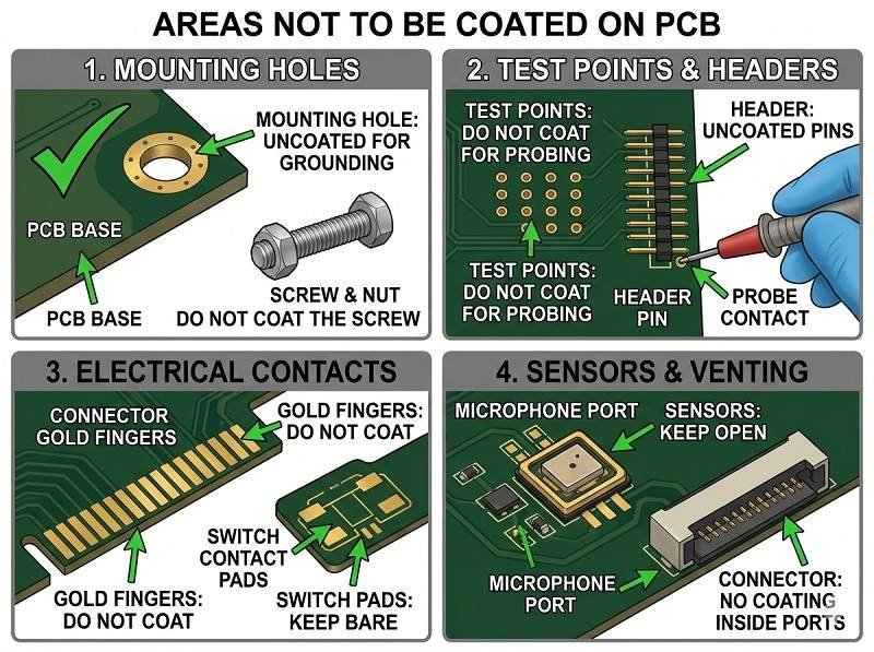
Aşağıda olması gereken kilit alanlar verilmiştir değil kaplanmalıdır:
Konektörler ve kontak pimleri
Tüm konektörler, kenar parmakları, soketler ve kontak pedleri kaplanmamış olarak kalmalıdır. Uygulama Konformal Kaplama bu yüzeylerde elektrik iletkenliğini engelleyebilir ve kablolar veya modüllerle düzgün eşleşmeyi önleyebilir. Bu, aşağıdakilerdeki en kritik maskeleme gereksinimlerinden biridir PCB Montajı.
Test noktaları ve programlama arayüzleri
Test pedleri, prob noktaları ve programlama başlıkları, elektrik testi, hata ayıklama ve ürün yazılımı güncellemelerine izin vermek için kaplamasız tutulmalıdır. İçinde Prototip PCB Montajı, bu noktalara erişim özellikle doğrulama ve sorun giderme için önemlidir.
Anahtarlar ve mekanik bileşenler
Düğmeler, röleler, atlama telleri ve diğer hareketli parçalar kaplanmamalıdır. Kaplama mekanik çalışmayı engelleyebilir veya bileşenlerin yapışmasına neden olarak işlevselliği azaltabilir. SMT Montajı ürünler.
Isı alıcıları ve termal arayüzler
Isı dağıtımı için tasarlanmış alanlar (ısı alıcıları, termal pedler veya güç bileşenleri gibi) tipik olarak kaplamasız kalmalı veya özel termal kaplamalar kullanılmalıdır. Standart kaplamalar ısı izolatörü görevi görerek ısı aktarım verimliliğini azaltabilir.
Yüksek gerilim boşlukları
Bazı yüksek voltajlı alanlarda güvenlik ve performans için kontrollü aralıklar gerekebilir. Kaplama yalıtımı iyileştirebilirken, yanlış uygulama boşlukları kapatabilir veya kirleticileri hapsederek güvenilirliği etkileyebilir. Uygulama sırasında dikkatli bir tasarım değerlendirmesi gereklidir. PCB Montajı.
Topraklama noktaları ve ekranlama alanları
Uygun elektromanyetik kalkanlama ve topraklama performansı sağlamak için metal kalkanlama bölgeleri veya topraklama kontakları açıkta kalmalıdır.
Yüksek frekanslı sinyaller için konektörler (RF alanları)
RF devrelerinde kaplama, empedansı veya sinyal özelliklerini değiştirebilir. Antenler veya RF konektörleri gibi hassas alanların kaplanmadan kalması veya özel malzemeler gerektirmesi gerekebilir.
Optik bileşenler (LED'ler, sensörler)
LED lensler, optik sensörler ve ekran elemanları kaplanmamalıdır, çünkü kaplama ışık iletimini engelleyebilir veya bozabilir. İçinde SMT Montajı, Bu alanların maskelenmesi optik performansın korunması için çok önemlidir.
Doğru maskeleme neden önemlidir?
Bu alanların korunmaması aşağıdakilere yol açabilir:
- Kötü elektrik bağlantıları
- Test ve onarım zorluğu
- Bileşenlerin mekanik arızası
- Azaltılmış termal performans
İçinde Prototip PCB Montajı, mühendisleri genellikle maskeleme bölgelerini tasarım aşamasının başlarında tanımlar ve seri üretimden önce test ederek doğrular.
En iyi uygulamalar
- Dışarıda tutma bölgelerini tasarım dosyalarında açıkça işaretleyin
- Maskeleme bantları, botlar veya sıvı maskeler kullanın
- Hassasiyet için seçici kaplama uygulayın
- Temizliği doğrulamak için kaplama sonrası denetim gerçekleştirin
Sonuç olarak, bir PCB'nin tüm alanları kaplanmamalıdır. Kaplama sırasında hassas bölgelerin uygun şekilde tanımlanması ve korunması PCB Montajı, SMT Montajı, ve Prototip PCB Montajı sağlamak Konformal Kaplama işlevsellikten ödün vermeden güvenilirliği artırır.
Konformal Kaplama Teklifi Alın
Prototipten seri üretime kadar konformal kaplama hizmetleri sunuyoruz. Teklifinizi şimdi alın.
İhtiyaçlarınızı bize gönderin ve mühendislik ekibimizden hızlı bir yanıt alın.
✔ 24 saat yanıt ✔ Mühendislik desteği ✔ Küçük ve Seri Üretim
Shenzhen Tengxinjie Electronics Co, Ltd.


