SMT Process Flow
Сайт SMT process flow refers to the complete sequence of steps used in Сборка SMT (Surface Mount Technology) to mount electronic components directly onto the surface of a printed circuit board. It is the most widely used method in modern Сборка печатной платы, known for its speed, precision, and suitability for high-density electronic products.
Below is a detailed, real-world explanation of the SMT process flow used in professional PCB manufacturing.
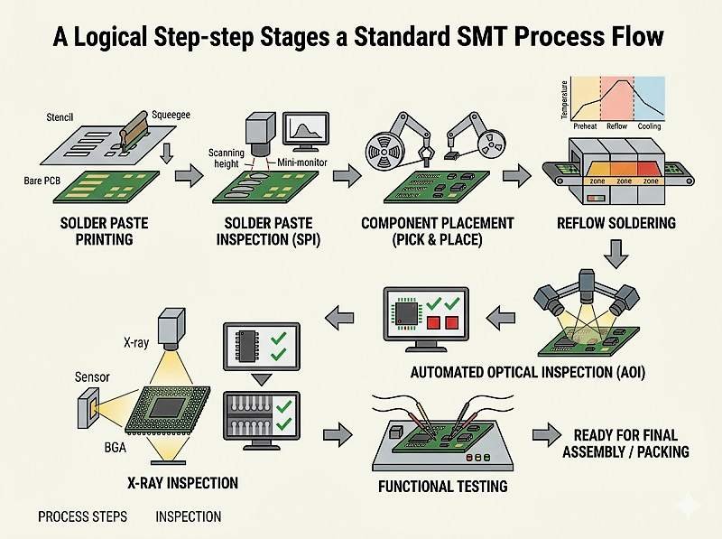
Overview of SMT Process Flow
A standard SMT Assembly process typically includes:
- Solder paste inspection (optional but recommended)
- Solder paste printing
- SPI (контроль паяльной пасты)
- Pick-and-place (component placement)
- Пайка оплавлением
- AOI (автоматизированная оптическая инспекция)
- X-ray inspection (if required)
- Cleaning and repair (if needed)
Each step plays a critical role in ensuring high-quality PCB Assembly.
Печать паяльной пастой
This is the first and most critical step in SMT Assembly:
- A stencil is aligned over the PCB
- Solder paste is applied to component pads
- Paste consists of solder particles and flux
Key control points:
- Stencil thickness
- Printing pressure
- Alignment accuracy
Defects at this stage can affect the entire SMT process.
Контроль паяльной пасты (SPI)
After printing, SPI systems check the quality of the paste:
- Measures paste volume, height, and alignment
- Detects insufficient or excessive solder
- Prevents defects early in PCB Assembly
SPI significantly improves yield and reduces rework.
Pick-and-Place (Component Placement)
In this stage of SMT Assembly:
- Automated machines place components onto the PCB
- Components are picked from reels, trays, or tubes
- Vision systems ensure accurate alignment
Modern machines can place:
- Small passive components (0201, 01005)
- Complex ICs (QFP, BGA)
This step determines placement accuracy and production speed.
Пайка оплавлением
After placement, boards go through a reflow oven:
- Controlled heating melts solder paste
- Components are permanently soldered
- Cooling solidifies the joints
Reflow stages include:
- Preheating
- Soaking
- Reflow peak
- Охлаждение
Proper temperature profiling is essential to avoid defects.
AOI (автоматизированная оптическая инспекция)
After soldering, AOI systems inspect the board:
- Detects missing or misaligned components
- Identifies soldering defects (bridges, insufficient solder)
- Ensures overall assembly quality
AOI is a standard step in high-quality PCB Assembly lines.
X-ray Inspection (For Complex Components)
For hidden solder joints (e.g., BGA):
- X-ray inspection is used
- Detects internal defects such as voids or bridging
This step is critical for advanced SMT Assembly projects.
Cleaning Process (Optional)
Depending on requirements:
- Flux residues may be removed
- Cleaning improves reliability, especially in sensitive applications
Not all PCB Assembly processes require cleaning.
Переделка и ремонт
If defects are found:
- Manual or automated rework is performed
- Components may be replaced or resoldered
Rework ensures final product quality meets standards.
Final Inspection and Quality Assurance
Before completion:
- Визуальный осмотр
- Electrical testing (optional)
- Quality verification
This ensures the SMT Assembly meets all specifications.
Key Factors Affecting SMT Process Flow
- PCB design quality
- Component type and size
- Solder paste quality
- Machine precision
- Process control and environment
Proper optimization improves yield and reduces defects.
Advantages of SMT Assembly Process
- High automation and efficiency
- Suitable for high-density designs
- Lower labor cost
- Более высокая скорость производства
- Better electrical performance
This is why SMT Assembly dominates modern PCB manufacturing.
Common SMT Defects
- Томбстоунинг
- Solder bridging
- Cold joints
- Misalignment
- Insufficient solder
Most defects originate from poor process control or design issues.
Заключение
The SMT process flow is a highly automated and precise sequence that forms the backbone of modern Сборка печатной платы. From solder paste printing to final inspection, each step in Сборка SMT is critical to ensuring product quality and reliability.
Understanding this process helps engineers and buyers optimize design, reduce defects, and improve overall manufacturing efficiency.
Планируете следующий проект по электронике? Начните с предложения по сборке печатной платы.
Мы предоставляем профессиональные услуги по сборке печатных плат, включая SMT, DIP и полные решения "под ключ".
✔ NDA доступно ✔ Быстрая котировка в течение 24 часов ✔ ISO сертифицированный завод ✔ Одна остановка PCB & PCBA службы


