Export Gerber Files from Altium Designer
Exporting Gerber files from Altium Designer is a key step in preparing your design for Производство печатных плат и Сборка печатной платы. These files ensure your board layout is correctly translated into fabrication data for Сборка SMT и Сборка печатных плат под ключ.
Below is a step-by-step guide to exporting Gerber files properly.
Step 1: Open Your PCB Project
Start by opening your completed PCB layout file (.PcbDoc) in Altium Designer.
Before exporting, make sure your design is finalized and has passed all design rule checks (DRC). This helps prevent errors during PCB Manufacturing.
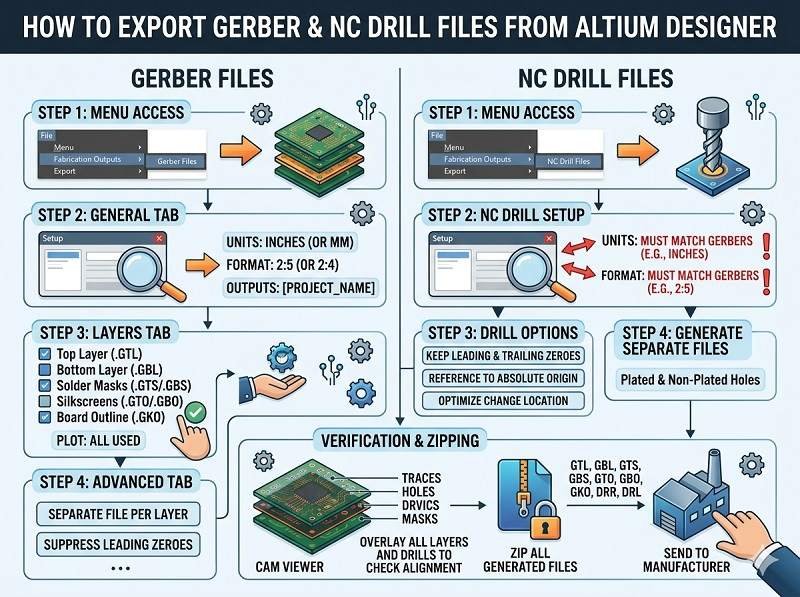
Step 2: Open the Gerber Export Tool
Go to the top menu:
File → Fabrication Outputs → Gerber Files
This will open the Gerber setup window where you can configure export settings.
Step 3: Configure General Settings
In the “General” tab:
- Set Units (millimeters or inches, mm is recommended)
- Выберите Format (e.g., 2:5 or 2:6 precision)
- Select RS-274X format (industry standard)
- Enable Embedded apertures
These settings ensure compatibility with most Производство печатных плат процессы.
Step 4: Select Layers to Export
Switch to the “Layers” tab and select all required layers.
Typical layers include:
- Top Layer (Top Copper)
- Bottom Layer (Bottom Copper)
- Internal Layers (for multilayer PCBs)
- Top Solder Mask
- Bottom Solder Mask
- Top Silkscreen (Overlay)
- Bottom Silkscreen
- Board Outline (Mechanical Layer)
Selecting the correct layers is critical for accurate Сборка печатной платы and fabrication.
Step 5: Configure Apertures and Advanced Settings
In the “Apertures” tab:
- Используйте Embedded apertures (RS-274X)
In advanced settings:
- Enable Plot Layers in correct order
- Mirror settings only if required (usually off for standard exports)
Step 6: Generate Gerber Files
Click OK to generate the Gerber files.
Altium will output a set of files, each representing a PCB layer. These files will be saved in your project’s output folder.
Step 7: Export NC Drill Files
Gerber files alone are not enough—you also need drill data.
Go to:
File → Fabrication Outputs → NC Drill Files
Configure:
- Units (same as Gerber)
- Format (match Gerber precision)
Export the drill file, which defines hole locations and sizes for Производство печатных плат.
Step 8: Verify Gerber Files
Before sending files for Сборка печатной платы, always verify them using a Gerber viewer (Altium has a built-in viewer or you can use third-party tools).
Check for:
- Missing layers
- Alignment issues
- Correct board outline
- Proper pad and mask openings
This step helps avoid costly errors in Сборка SMT и производство.
Step 9: Prepare for Turnkey PCB Assembly
Для Сборка печатных плат под ключ, you will need to provide:
- Файлы Gerber
- Файлы для сверления с ЧПУ
- BOM (спецификация материалов)
- Pick and place (centroid) file
- Сборочные чертежи
A complete file package ensures smooth coordination between PCB Manufacturing and assembly.
Common Mistakes to Avoid
- Exporting in outdated Gerber formats (always use RS-274X)
- Forgetting solder mask or silkscreen layers
- Mismatched units between Gerber and drill files
- Missing board outline
- Not verifying files before submission
Avoiding these mistakes ensures a smoother manufacturing process.
Заключение
Exporting Gerber files from Altium Designer is a straightforward but critical step in PCB production. By correctly configuring settings, selecting the right layers, and verifying outputs, you can ensure high-quality results in Производство печатных плат, Сборка SMT, и Сборка печатных плат под ключ.
A well-prepared Gerber package minimizes errors, reduces delays, and helps deliver reliable electronic products.
Получите квалифицированную консультацию и точную цену за один шаг. Запросите цену сегодня.
Мы предоставляем профессиональные услуги по сборке печатных плат, включая SMT, DIP и полные решения "под ключ".
✔ NDA доступно ✔ Быстрая котировка в течение 24 часов ✔ ISO сертифицированный завод ✔ Одна остановка PCB & PCBA службы


