PCB Stencil
A PCB stencil is a thin sheet, typically made of stainless steel or nickel, used in the Montaż SMT process to apply solder paste accurately onto a printed circuit board (PCB). It contains precisely cut openings that match the solder pads on the PCB, allowing controlled deposition of solder paste before component placement.
PCB stencils are essential tools in modern Montaż PCB, ensuring consistency, accuracy, and high-quality solder joints, especially for fine-pitch and high-density designs.
How a PCB Stencil Works
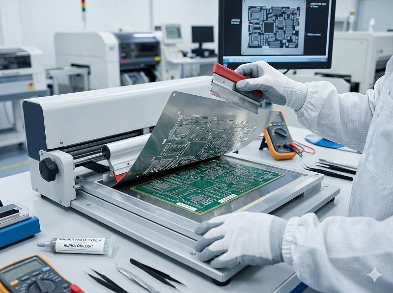
During the SMT Assembly process, the PCB is aligned over the bare PCB. Solder paste is then spread across the stencil using a squeegee. The paste passes through the stencil apertures and deposits onto the exposed pads of the PCB.
Once the stencil is removed, the solder paste remains only on the intended areas. Components are then placed onto the paste, and the board is sent through a reflow oven where the solder melts and forms solid electrical connections.
This process is a critical step bridging Produkcja obwodów drukowanych and PCB Assembly, ensuring that components are mounted accurately and reliably.
Types of PCB Stencils
There are several types of PCB stencils used depending on production requirements.
Framed stencils are mounted in a rigid frame, making them suitable for high-volume production and automated SMT Assembly lines. They provide stability and repeatability.
Frameless stencils, also known as foil stencils, are more flexible and cost-effective. They are often used in prototyping or low-volume Montaż PCB.
Prototype stencils are designed for quick turnaround and small batches. They are commonly used during product development and testing phases.
Electroformed stencils offer high precision and are used for ultra-fine pitch components, where accuracy is critical.
Materials Used in PCB Stencils
Most PCB stencils are made from stainless steel due to its durability, flexibility, and resistance to wear. For high-precision applications, nickel electroformed stencils may be used to achieve smoother aperture walls and better paste release.
The thickness of the stencil is also important, as it determines the volume of solder paste deposited. Choosing the correct thickness is essential for achieving reliable solder joints.
Importance of PCB Stencils in SMT Assembly
PCB stencils play a vital role in ensuring consistent solder paste application. Without a stencil, it would be extremely difficult to control the amount and placement of solder paste, leading to defects such as solder bridges, insufficient solder, or misalignment.
In automated SMT Assembly, stencils enable high-speed and repeatable processes, which are essential for both low-volume and high-volume production.
They also contribute to overall product quality by improving solder joint reliability, which directly impacts the performance and lifespan of electronic devices.
PCB Stencil Design Considerations
Designing an effective PCB stencil requires careful consideration of several factors.
Aperture size and shape must match the PCB pad design to ensure proper paste deposition. Adjustments may be needed for fine-pitch components or specific package types.
Stencil thickness must be selected based on component size and board complexity. Thinner stencils are used for fine-pitch designs, while thicker stencils are suitable for larger components.
Surface finish and coating can also affect paste release and cleaning efficiency. Smooth surfaces help improve printing performance and reduce defects.
PCB Stencil in Turnkey PCB Assembly
W Montaż płytek drukowanych pod klucz, the manufacturer typically handles stencil design and fabrication as part of the overall service. This ensures compatibility between PCB Manufacturing, stencil design, and SMT Assembly processes.
By integrating stencil production into the workflow, manufacturers can optimize solder paste application and reduce errors, leading to better overall assembly quality.
Common Issues Related to PCB Stencils
Despite their importance, PCB stencils can present challenges if not properly designed or maintained.
Common issues include clogged apertures, misalignment, and excessive or insufficient solder paste deposition. Regular cleaning and proper handling are essential to maintain stencil performance.
Improper stencil design can also lead to defects such as tombstoning, bridging, or poor solder joints.
Wnioski
A PCB stencil is a fundamental tool in the SMT Assembly process, enabling precise and consistent solder paste application. It plays a crucial role in ensuring high-quality PCB Assembly and reliable electronic performance.
When combined with optimized PCB Manufacturing and Turnkey PCB Assembly services, a well-designed stencil helps improve efficiency, reduce defects, and support both prototyping and high-volume production.
Prześlij swoje pliki i otrzymaj szczegółową wycenę. Kliknij poniżej, aby rozpocząć.
Zapewniamy profesjonalne usługi montażu PCB, w tym SMT, DIP i pełne rozwiązania "pod klucz".
✔ Dostępna NDA ✔ Szybka wycena w ciągu 24 godzin ✔ Fabryka z certyfikatem ISO ✔ Kompleksowy serwis PCB i PCBA


