솔더 페이스트 인쇄
Solder paste printing is the first and one of the most critical steps in PCB 어셈블리, especially in modern SMT 어셈블리 processes. It involves applying a precise amount of solder paste onto the pads of a printed circuit board (PCB) to prepare it for component placement and soldering.
The quality of solder paste printing directly affects the success of the entire PCB Assembly process, making it a key factor in achieving high yield and reliable products.
What is Solder Paste?
Solder paste is a mixture of:
- Metal solder particles (typically tin-based alloys)
- Flux (a chemical agent that removes oxidation and improves soldering)
This paste is used to temporarily hold components in place and create strong electrical and mechanical connections after reflow.
Solder Paste Printing Process Overview
The solder paste printing process in SMT 어셈블리 typically includes:
- Stencil alignment
- Paste application
- Squeegee printing
- Stencil separation
Each step must be precisely controlled to ensure accurate paste deposition.
Step-by-Step Solder Paste Printing Process
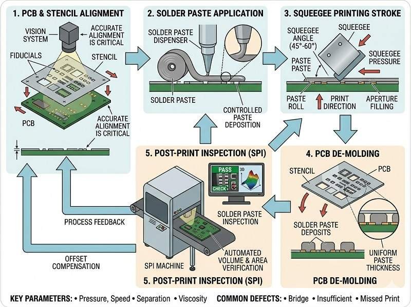
Stencil Alignment
- A 스테인리스 스틸 스텐실 is placed over the PCB
- Openings in the stencil correspond to solder pads
- Accurate alignment ensures correct paste placement
Misalignment can lead to solder defects later in PCB Assembly.
Paste Application
- Solder paste is placed on top of the stencil
- The amount of paste must be carefully controlled
Too much or too little paste can cause defects such as bridging or weak joints.
Squeegee Printing
- A squeegee blade moves across the stencil
- Paste is pushed into stencil openings
- Excess paste is removed
This step determines the volume and consistency of solder paste deposits.
Stencil Separation
- The stencil is lifted from the PCB
- Paste remains on the pads in precise shapes
Proper separation ensures clean edges and accurate deposition.
Why Solder Paste Printing is Important
Solder paste printing is critical because it directly affects:
- Solder joint quality
- Component placement stability
- Electrical connectivity
- Overall PCB Assembly yield
👉 Most SMT defects originate from poor solder paste printing.
Key Parameters in Solder Paste Printing
Several factors influence printing quality:
- Stencil thickness and design
- Squeegee pressure and speed
- Paste viscosity and temperature
- Environmental conditions (humidity, temperature)
Optimizing these parameters is essential for consistent SMT 어셈블리 results.
Common Solder Paste Printing Defects
- Insufficient solder: weak joints
- Excess solder: bridging or shorts
- Misalignment: poor component placement
- Slumping: paste spreading before reflow
- Voiding: air gaps in solder joints
Most of these issues can be detected early using inspection systems.
솔더 페이스트 검사(SPI)
After printing, many PCB Assembly lines use SPI systems:
- Measures paste volume and height
- Detects printing defects early
- Improves yield and reduces rework
SPI is a standard quality control step in advanced SMT Assembly.
Types of Solder Paste
Common solder paste types include:
- Lead-free (RoHS compliant)
- No-clean paste (minimal residue)
- Water-soluble paste (requires cleaning)
The choice depends on product requirements and environmental standards.
How to Optimize Solder Paste Printing
To improve PCB Assembly quality:
- Use high-quality stencil design
- Maintain proper paste storage and handling
- Calibrate printing equipment regularly
- 환경 조건 제어
- Implement SPI inspection
결론
Solder paste printing is a foundational step in PCB 어셈블리 그리고 SMT 어셈블리, directly influencing the quality of solder joints and overall product reliability. A well-controlled printing process ensures accurate paste deposition, reduces defects, and improves manufacturing efficiency.
Understanding and optimizing this step is essential for achieving high-quality PCB Assembly results.
파일을 업로드하고 자세한 견적을 받아보세요. 시작하려면 아래를 클릭하세요.
당사는 SMT, DIP 및 전체 턴키 솔루션을 포함한 전문 PCB 조립 서비스를 제공합니다.
NDA 가능 ✔ 24시간 이내 빠른 견적 ✔ ISO 인증 공장 ✔ 원스톱 PCB 및 PCBA 서비스


