Покрытие на печатной плате
Во время Конформное покрытие в Сборка печатной платы, Сборка прототипа печатной платы, и Сборка SMT, необходимо определить запретные зоны-области, которые должны оставаться свободными от покрытия, чтобы обеспечить надлежащие электрические характеристики, связь и возможность обслуживания. Нанесение покрытия на неправильные участки может привести к плохому контакту, проблемам с сигналом или даже к полному отказу изделия.
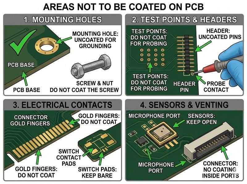
Ниже перечислены ключевые области, которые должны не быть покрыты:
Разъемы и контактные штыри
Все разъемы, краевые пальцы, гнезда и контактные площадки должны оставаться без покрытия. Нанесение Конформное покрытие на этих поверхностях может блокировать электропроводность и препятствовать правильному сопряжению с кабелями или модулями. Это одно из наиболее важных требований к маскировке в Сборка печатной платы.
Тестовые точки и программные интерфейсы
Тестовые площадки, точки подключения датчиков и программирующие головки должны быть свободны от покрытия, чтобы можно было проводить электрические испытания, отладку и обновление прошивки. На сайте Сборка прототипа печатной платы, Доступ к этим точкам особенно важен для проверки и устранения неполадок.
Переключатели и механические компоненты
Кнопки, реле, перемычки и другие подвижные детали не следует покрывать лаком. Покрытие может помешать механической работе или привести к прилипанию компонентов, что снизит функциональность. Сборка SMT продукты.
Теплоотводы и термоинтерфейсы
Участки, предназначенные для отвода тепла, такие как радиаторы, термопрокладки или силовые компоненты, обычно остаются без покрытия или используют специализированные термопокрытия. Стандартные покрытия могут выступать в качестве теплоизоляторов, снижая эффективность теплопередачи.
Высоковольтные зазоры
В некоторых высоковольтных зонах может потребоваться контролируемое расстояние для обеспечения безопасности и производительности. Хотя покрытие может улучшить изоляцию, неправильное нанесение может привести к образованию зазоров или скоплению загрязнений, что негативно скажется на надежности. Необходимо тщательно продумать конструкцию при Сборка печатной платы.
Точки заземления и зоны экранирования
Металлические экранирующие зоны или заземляющие контакты должны оставаться открытыми для обеспечения надлежащего электромагнитного экранирования и заземления.
Разъемы для высокочастотных сигналов (радиочастотные зоны)
В радиочастотных цепях покрытие может изменить импеданс или характеристики сигнала. Чувствительные участки, такие как антенны или ВЧ-разъемы, могут остаться без покрытия или потребовать применения специальных материалов.
Оптические компоненты (светодиоды, датчики)
На светодиодные линзы, оптические датчики и элементы дисплея не следует наносить покрытие, так как оно может блокировать или искажать передачу света. На сайте Сборка SMT, Маскировка этих областей имеет решающее значение для сохранения оптических характеристик.
Почему правильная маскировка имеет значение
Неспособность защитить эти зоны может привести к:
- Плохие электрические соединения
- Сложность тестирования и ремонта
- Механический отказ компонентов
- Снижение тепловых характеристик
На сайте Сборка прототипа печатной платы, Инженеры обычно определяют зоны маскировки на ранних этапах проектирования и проверяют их в ходе испытаний перед началом серийного производства.
Лучшие практики
- Четко обозначьте зоны несанкционированного доступа в проектных файлах
- Используйте маскировочные ленты, сапоги или жидкие маски.
- Нанесение селективного покрытия для обеспечения точности
- Выполните проверку чистоты после нанесения покрытия
В заключение следует отметить, что не все участки печатной платы должны покрываться лаком. Правильная идентификация и защита чувствительных зон во время Сборка печатной платы, Сборка SMT, и Сборка прототипа печатной платы обеспечивать, чтобы Конформное покрытие повышает надежность без ущерба для функциональности.
Получить цитату о конформном покрытии
Мы предоставляем услуги по нанесению конформного покрытия от прототипа до серийного производства. Получите ваше предложение прямо сейчас.
Отправьте нам свои требования и получите быстрый ответ от нашей команды инженеров.
✔ Круглосуточное реагирование ✔ Инженерная поддержка ✔ Мелкое и массовое производство
Shenzhen Tengxinjie Electronics Co., Ltd.


