Revestido em PCB
Durante Revestimento conformacional em Montagem de PCB, Montagem de protótipo de PCB, e Montagem SMT, é essencial definir áreas de exclusão-regiões que devem permanecer livres de revestimento para garantir o desempenho elétrico, a conectividade e a facilidade de manutenção adequados. O revestimento das áreas erradas pode causar mau contato, problemas de sinal ou até mesmo a falha total do produto.
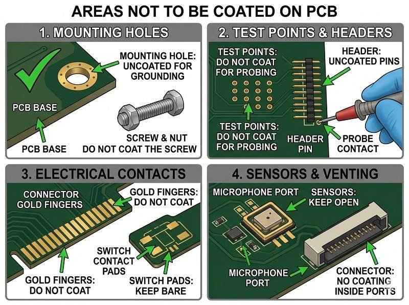
Abaixo estão as principais áreas que devem não ser revestido:
Conectores e pinos de contato
Todos os conectores, dedos de borda, soquetes e almofadas de contato devem permanecer sem revestimento. Aplicação de Revestimento conformacional nessas superfícies podem bloquear a condutividade elétrica e impedir o acoplamento adequado com cabos ou módulos. Esse é um dos requisitos de mascaramento mais críticos em Montagem de PCB.
Pontos de teste e interfaces de programação
As almofadas de teste, os pontos de sonda e os cabeçalhos de programação devem ser mantidos livres de revestimento para permitir testes elétricos, depuração e atualizações de firmware. Em Montagem de protótipo de PCB, O acesso a esses pontos é especialmente importante para validação e solução de problemas.
Interruptores e componentes mecânicos
Botões, relés, jumpers e outras peças móveis não devem ser revestidos. O revestimento pode interferir na operação mecânica ou fazer com que os componentes grudem, reduzindo a funcionalidade em Montagem SMT produtos.
Dissipadores de calor e interfaces térmicas
As áreas projetadas para dissipação de calor - como dissipadores de calor, almofadas térmicas ou componentes de potência - normalmente não devem ser revestidas ou devem usar revestimentos térmicos especializados. Os revestimentos padrão podem atuar como isolantes térmicos, reduzindo a eficiência da transferência de calor.
Folgas de alta tensão
Certas áreas de alta tensão podem exigir espaçamento controlado para segurança e desempenho. Embora o revestimento possa melhorar o isolamento, a aplicação inadequada pode preencher lacunas ou prender contaminantes, afetando a confiabilidade. É necessária uma consideração cuidadosa do projeto durante Montagem de PCB.
Pontos de aterramento e áreas de blindagem
As zonas de blindagem de metal ou os contatos de aterramento devem permanecer expostos para garantir o desempenho adequado da blindagem eletromagnética e do aterramento.
Conectores para sinais de alta frequência (áreas de RF)
Nos circuitos de RF, o revestimento pode alterar a impedância ou as características do sinal. Áreas sensíveis, como antenas ou conectores de RF, podem precisar permanecer sem revestimento ou exigir materiais especializados.
Componentes ópticos (LEDs, sensores)
As lentes de LED, os sensores ópticos e os elementos de tela não devem ser revestidos, pois o revestimento pode bloquear ou distorcer a transmissão de luz. Em Montagem SMT, Por isso, mascarar essas áreas é fundamental para manter o desempenho óptico.
Por que o mascaramento adequado é importante
Deixar de proteger essas áreas pode levar a:
- Conexões elétricas ruins
- Dificuldade de teste e reparo
- Falha mecânica de componentes
- Desempenho térmico reduzido
Em Montagem de protótipo de PCB, Em geral, os engenheiros definem as zonas de mascaramento no início da fase de projeto e as validam por meio de testes antes da produção em massa.
Práticas recomendadas
- Marque claramente as zonas de exclusão nos arquivos de projeto
- Use fitas adesivas, botas ou máscaras líquidas
- Aplique revestimento seletivo para obter precisão
- Realizar inspeção pós-revestimento para verificar a limpeza
Em conclusão, nem todas as áreas de um PCB devem ser revestidas. A identificação e a proteção adequadas das zonas sensíveis durante o processo de revestimento devem ser feitas com cuidado. Montagem de PCB, Montagem SMT, e Montagem de protótipo de PCB garantir que Revestimento conformacional aumenta a confiabilidade sem comprometer a funcionalidade.
Obter uma cotação de revestimento isolante
Do protótipo à produção em massa, fornecemos serviços de revestimento isolante. Obtenha sua cotação agora.
Envie-nos seus requisitos e receba uma resposta rápida de nossa equipe de engenharia.
Resposta 24 horas ✔ Suporte de engenharia ✔ Produção pequena e em massa
Shenzhen Tengxinjie Electronics Co., Ltd.


