BGA Soldering Process
The BGA (Ball Grid Array) soldering process is a specialized technique in Montaż PCB used to mount BGA components onto a printed circuit board. Unlike traditional packages, BGA components have solder balls arranged in a grid underneath the device, making the solder joints hidden from view. This process is widely used in advanced Montaż SMT due to its ability to support high-density and high-performance electronic designs.
What is a BGA Component?
A BGA package consists of:
- An integrated circuit (IC)
- An array of solder balls on the bottom surface
- A substrate that connects the chip to the solder balls
👉 These solder balls act as both electrical connections and mechanical support during Montaż PCB.
Why BGA is Used in SMT Assembly
BGA components offer several advantages:
- Higher pin density compared to traditional packages
- Better electrical performance (shorter signal paths)
- Improved heat dissipation
- Reduced board space
👉 This makes BGA ideal for modern electronics like smartphones, computers, and industrial devices.
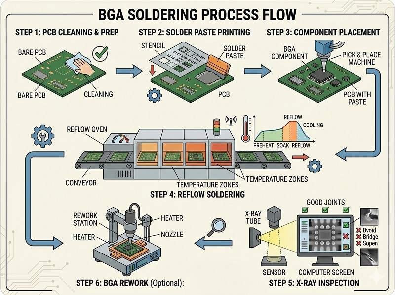
BGA Soldering Process Steps
Drukowanie pasty lutowniczej
- Solder paste is applied to PCB pads using a stencil
- Accurate volume control is critical
Rozmieszczenie komponentów
- BGA is placed using high-precision pick-and-place machines
- Alignment is crucial since joints are hidden
Lutowanie rozpływowe
- The PCB passes through a reflow oven
- Heat melts the solder balls and paste
- Surface tension helps self-align the component
👉 Proper temperature control is essential in Montaż SMT.
Chłodzenie
- Controlled cooling solidifies solder joints
- Prevents defects like cracks or warping
Kontrola
- X-ray inspection is used to check hidden solder joints
- Ensures connection quality and detects defects
Reflow Profile for BGA
A typical BGA reflow profile includes:
- Preheat stage – Gradual temperature rise
- Soak stage – Activates flux and stabilizes temperature
- Reflow stage – Solder melts (typically 217–245°C for lead-free)
- Cooling stage – Controlled solidification
👉 Optimizing the profile is critical for reliable Montaż PCB.
Common BGA Soldering Defects
BGA soldering can produce defects such as:
- Voids in solder joints
- Head-in-pillow defects
- Bridging between balls
- Open connections
- Misalignment
👉 These defects are difficult to detect without X-ray inspection.
Challenges in BGA Soldering
- Hidden solder joints
- Tight process control requirements
- Sensitivity to temperature and moisture
- Difficulty in rework and repair
BGA Rework Process
If defects occur, BGA components can be reworked:
- Remove the faulty component using controlled heating
- Clean residual solder from pads
- Reball the component (if needed)
- Replace and reflow the component
👉 Rework requires specialized equipment and expertise.
Advantages of BGA Soldering
- Supports high-density PCB designs
- Reliable electrical connections
- Better thermal performance
- Compact and efficient layout
Limitations of BGA Soldering
- Requires advanced inspection (X-ray)
- Higher manufacturing complexity
- Difficult rework process
- Strict process control needed
Applications of BGA in PCB Assembly
BGA soldering is widely used in:
- Consumer electronics (smartphones, laptops)
- Systemy motoryzacyjne
- Przemysłowe płyty sterujące
- Sprzęt telekomunikacyjny
Best Practices for BGA Soldering
- Optimize stencil design and solder paste volume
- Use accurate pick-and-place alignment
- Develop proper reflow temperature profiles
- Control moisture sensitivity (MSL handling)
- Use X-ray inspection for quality assurance
Role in PCB Assembly
W nowoczesnym Montaż PCB oraz Montaż SMT, BGA soldering is essential for achieving compact, high-performance designs. It represents a key capability for advanced electronics manufacturing.
Wnioski
The BGA soldering process is a fundamental part of advanced Montaż PCB, enabling high-density and high-performance electronic designs. With precise control over placement, reflow, and inspection, manufacturers can achieve reliable solder joints even in complex Montaż SMT aplikacje.
Masz na myśli projekt PCB? Poproś o wycenę i uzyskaj wsparcie ekspertów już dziś.
Zapewniamy profesjonalne usługi montażu PCB, w tym SMT, DIP i pełne rozwiązania "pod klucz".
✔ Dostępna NDA ✔ Szybka wycena w ciągu 24 godzin ✔ Fabryka z certyfikatem ISO ✔ Kompleksowy serwis PCB i PCBA


