Powlekane na płytce drukowanej
Podczas Powłoka konformalna w Montaż PCB, Montaż prototypów PCB, oraz Montaż SMT, konieczne jest zdefiniowanie obszary zakazu wstępu-Obszary, które muszą pozostać wolne od powłoki, aby zapewnić odpowiednią wydajność elektryczną, łączność i łatwość serwisowania. Powlekanie niewłaściwych obszarów może prowadzić do słabego kontaktu, problemów z sygnałem, a nawet całkowitej awarii produktu.
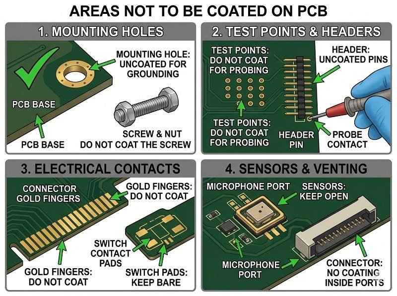
Poniżej znajdują się kluczowe obszary, które powinny nie być powlekane:
Złącza i styki kontaktowe
Wszystkie złącza, palce krawędziowe, gniazda i podkładki stykowe muszą pozostać niepowleczone. Stosowanie Powłoka konformalna na tych powierzchniach może blokować przewodność elektryczną i uniemożliwiać prawidłowe połączenie z kablami lub modułami. Jest to jeden z najbardziej krytycznych wymogów dotyczących maskowania w Montaż PCB.
Punkty testowe i interfejsy programowania
Pady testowe, punkty sondy i nagłówki programowania powinny być wolne od powłoki, aby umożliwić testowanie elektryczne, debugowanie i aktualizacje oprogramowania układowego. W Montaż prototypów PCB, Dostęp do tych punktów jest szczególnie ważny dla walidacji i rozwiązywania problemów.
Przełączniki i komponenty mechaniczne
Przyciski, przekaźniki, zworki i inne ruchome części nie powinny być powlekane. Powłoka może zakłócać działanie mechaniczne lub powodować przyklejanie się komponentów, zmniejszając funkcjonalność w Montaż SMT produkty.
Radiatory i interfejsy termiczne
Obszary przeznaczone do rozpraszania ciepła - takie jak radiatory, podkładki termiczne lub komponenty zasilające - powinny zazwyczaj pozostać niepowlekane lub wykorzystywać specjalistyczne powłoki termiczne. Standardowe powłoki mogą działać jako izolatory termiczne, zmniejszając wydajność wymiany ciepła.
Szczeliny wysokiego napięcia
Niektóre obszary wysokiego napięcia mogą wymagać kontrolowanych odstępów w celu zapewnienia bezpieczeństwa i wydajności. Podczas gdy powłoka może poprawić izolację, niewłaściwa aplikacja może wypełnić luki lub uwięzić zanieczyszczenia, wpływając na niezawodność. Konieczne jest staranne rozważenie projektu podczas Montaż PCB.
Punkty uziemienia i obszary ekranowania
Metalowe strefy ekranowania lub styki uziemienia powinny pozostać odsłonięte, aby zapewnić prawidłowe ekranowanie elektromagnetyczne i uziemienie.
Złącza dla sygnałów wysokiej częstotliwości (obszary RF)
W obwodach RF powłoka może zmieniać impedancję lub charakterystykę sygnału. Wrażliwe obszary, takie jak anteny lub złącza RF, mogą wymagać pozostawienia bez powłoki lub zastosowania specjalistycznych materiałów.
Komponenty optyczne (diody LED, czujniki)
Soczewki LED, czujniki optyczne i elementy wyświetlacza nie powinny być powlekane, ponieważ powłoka może blokować lub zniekształcać transmisję światła. W Montaż SMT, Maskowanie tych obszarów ma kluczowe znaczenie dla utrzymania wydajności optycznej.
Dlaczego właściwe maskowanie ma znaczenie
Brak ochrony tych obszarów może prowadzić do:
- Słabe połączenia elektryczne
- Trudności w testowaniu i naprawie
- Awaria mechaniczna podzespołów
- Zmniejszona wydajność termiczna
W Montaż prototypów PCB, Inżynierowie zazwyczaj definiują strefy maskowania na wczesnym etapie projektowania i zatwierdzają je poprzez testy przed masową produkcją.
Najlepsze praktyki
- Wyraźne oznaczenie stref zamkniętych w plikach projektowych
- Używaj taśm maskujących, butów lub masek w płynie
- Nałożenie powłoki selektywnej zapewnia precyzję
- Przeprowadzenie kontroli po nałożeniu powłoki w celu sprawdzenia jej czystości
Podsumowując, nie wszystkie obszary PCB powinny być powlekane. Właściwa identyfikacja i ochrona wrażliwych stref podczas Montaż PCB, Montaż SMT, oraz Montaż prototypów PCB zapewnić, że Powłoka konformalna Zwiększa niezawodność bez uszczerbku dla funkcjonalności.
Uzyskaj wycenę powłoki konformalnej
Od prototypu do produkcji masowej, świadczymy usługi powlekania konforemnego. Uzyskaj wycenę już teraz.
Prześlij nam swoje wymagania i uzyskaj szybką odpowiedź od naszego zespołu inżynierów.
24-godzinna reakcja ✔ Wsparcie inżynieryjne ✔ Mała i masowa produkcja
Shenzhen Tengxinjie Electronics Co., Ltd.


