PCB Depanelization
PCB depanelization is the process of separating individual printed circuit boards from a larger panel after Assemblage du circuit imprimé et Assemblage SMT are completed. During Fabrication de circuits imprimés, multiple PCBs are often fabricated and assembled together in a single panel to improve efficiency. Depanelization is the final step that cuts or separates these boards into individual units.
Why PCB Depanelization Is Necessary
Panelization is widely used to optimize production.
It allows multiple boards to be processed simultaneously during Assemblage SMT.
It improves handling efficiency and machine throughput.
It reduces manufacturing costs.
However, once assembly is complete, each PCB must be separated for testing, enclosure integration, or shipping. This is where depanelization becomes essential in Assemblage de circuits imprimés clés en main.
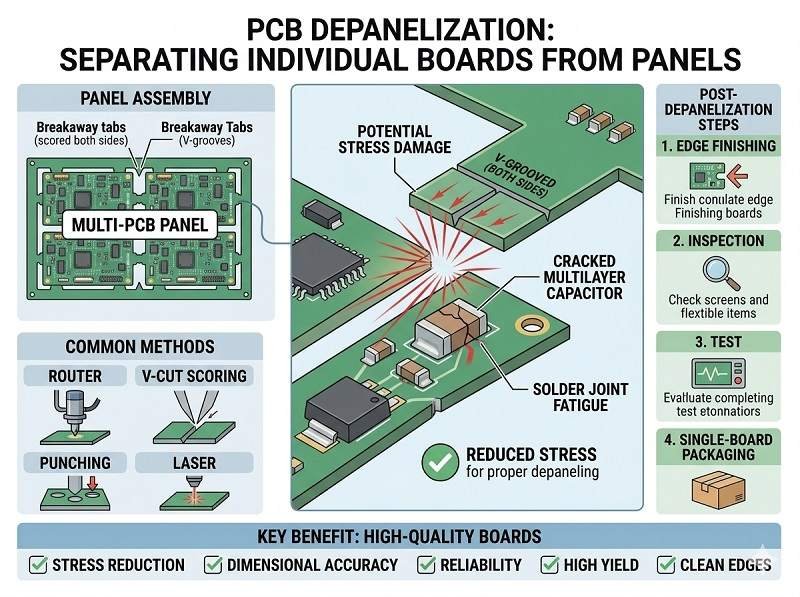
Common PCB Depanelization Methods
Different depanelization methods are used depending on board design, material, and production requirements.
V-Score (V-Cut) Depanelization
This method uses pre-scored lines on the PCB panel.
Boards are snapped apart manually or with a machine.
It is cost-effective and commonly used in high-volume Fabrication de circuits imprimés.
However, it may introduce mechanical stress if not handled properly.
Tab Routing (Mouse Bites)
Small tabs with perforated holes connect individual boards.
After assembly, the tabs are broken off.
This method provides better control than V-scoring and is suitable for irregular board shapes in Assemblage du circuit imprimé.
Router Depanelization
A CNC router cuts boards out of the panel.
It offers high precision and minimal stress on components.
This method is ideal for sensitive or high-density designs used in Assemblage SMT.
Laser Depanelization
A laser is used to separate boards without physical contact.
It produces very clean edges and minimal mechanical stress.
It is suitable for delicate PCBs and advanced applications in Assemblage de circuits imprimés clés en main.
Challenges in PCB Depanelization
Depanelization must be carefully controlled to avoid damage.
Mechanical stress can crack solder joints or damage components.
Improper handling can cause PCB warping.
Dust and debris may affect sensitive circuits.
These risks are especially critical in fine-pitch and high-density Assemblage SMT.
Best Practices for PCB Depanelization
To ensure high-quality results, manufacturers follow several best practices.
Choose the appropriate depanelization method based on PCB design.
Avoid placing sensitive components near board edges.
Use automated equipment for consistent results.
Control cutting speed and force to minimize stress.
Clean boards after depanelization if necessary.
Role in SMT and Turnkey PCB Assembly
En Assemblage SMT, depanelization is the final mechanical step after soldering and inspection.
En Assemblage de circuits imprimés clés en main, it is integrated into the overall production workflow, ensuring that finished boards are ready for final testing, packaging, or box build integration.
Conclusion
PCB depanelization is a crucial step in electronics manufacturing, converting assembled panels into individual PCBs ready for use. By selecting the right method and following best practices, manufacturers can minimize damage and maintain product quality.
En Assemblage du circuit imprimé, Assemblage SMT, et Assemblage de circuits imprimés clés en main, effective depanelization ensures that the final products meet both mechanical and electrical reliability requirements.
Vous planifiez votre prochain projet électronique ? Commencez par un devis d'assemblage de circuits imprimés.
Nous fournissons des services professionnels d'assemblage de circuits imprimés, y compris SMT, DIP et des solutions complètes clé en main.
✔ NDA disponible ✔ Devis rapide sous 24 heures ✔ Usine certifiée ISO ✔ Service unique de PCB et PCBA


