PCB Assembly Process
En Montaje de PCB process (PCBA) is the complete sequence of manufacturing steps used to mount, solder, and assemble electronic components onto a printed circuit board (PCB), transforming it into a fully functional electronic product. In modern electronics manufacturing, Montaje SMT (Surface Mount Technology) plays a dominant role due to its high efficiency, precision, and ability to support high-density designs.
A well-controlled PCB Assembly process ensures product reliability, electrical performance, and long-term durability. Below is a comprehensive, step-by-step explanation of how PCB Assembly works in real production environments.
Overview of the PCB Assembly Workflow
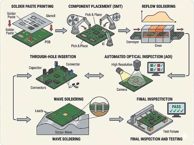
A standard PCB Assembly process typically includes the following stages:
- Design data preparation (DFM/DFA review)
- Solder paste printing
- SMT component placement
- Soldadura reflow
- Through-hole assembly (if required)
- Wave or selective soldering
- Inspección y control de calidad
- Cleaning and surface protection
- Functional testing and final inspection
Each stage must be carefully controlled to minimize defects and ensure consistent quality.
Design File Preparation and Engineering Review
Before production begins, manufacturers perform an engineering review:
- DFM (Design for Manufacturability) analysis
- DFA (Design for Assembly) checks
- Verification of Gerber files, BOM, and centroid data
This step ensures that the design is suitable for Montaje SMT and helps prevent costly production errors.
Impresión de pasta de soldadura
Solder paste printing is the first physical step in PCB Assembly:
- A stainless steel stencil is aligned with the PCB
- Solder paste is applied onto the pads
- The paste consists of solder alloy particles and flux
Key factors affecting quality:
- Stencil thickness
- Paste viscosity
- Printing alignment accuracy
Poor solder paste printing can lead to defects such as bridging or insufficient solder.
SMT Component Placement
En Montaje SMT, automated pick-and-place machines mount components onto the PCB:
- Components are picked from reels or trays
- Precisely placed onto solder paste-covered pads
- High-speed machines can place tens of thousands of components per hour
Modern SMT lines include:
- High-speed chip shooters
- Fine-pitch placement machines
- Sistemas de alineación visual
Accuracy at this stage is critical, especially for small packages like 0402, 0201, or BGA components.
Reflow Soldering Process
After placement, the PCB enters a reflow oven:
- The board passes through multiple temperature zones
- Solder paste melts and forms metallurgical bonds
- Controlled cooling solidifies the joints
Typical reflow profile stages:
- Preheat
- Soak
- Reflow
- Refrigeración
A properly controlled reflow process ensures strong, reliable solder joints and prevents issues such as tombstoning or cold joints.
Through-Hole Component Assembly
For boards requiring mechanical strength or specific components:
- Through-hole components are inserted into drilled holes
- This may be done manually or using insertion machines
Though less common than SMT, through-hole assembly is still important for connectors, transformers, and high-power components.
Wave Soldering and Selective Soldering
To solder through-hole components:
- Soldadura por ola passes the PCB over a موجة من solder molten
- Soldadura selectiva targets specific areas with precision
Selective soldering is preferred for mixed PCB Assembly where SMT components are already mounted.
Inspección y control de calidad
Quality assurance is critical throughout the PCB Assembly process. Common inspection methods include:
- AOI (Automated Optical Inspection): detects placement and soldering defects
- X-ray inspection: used for hidden joints (e.g., BGA, QFN)
- SPI (Solder Paste Inspection): checks paste volume and alignment
These inspections ensure that defects are identified early, reducing rework cost.
Cleaning and Surface Protection
After soldering, cleaning may be required:
- Removal of flux residues
- Use of deionized water or chemical cleaning agents
Optional protective processes include:
- Conformal coating (moisture and dust protection)
- Potting or encapsulation
These processes improve product reliability in harsh environments.
Functional Testing and Validation
Once assembly is complete, boards undergo testing:
- Functional testing (FCT): verifies real-world operation
- ICT (In-Circuit Testing): checks electrical connections
- Power-on testing and debugging
Testing ensures that the final product meets design specifications and performs correctly.
Types of PCB Assembly Processes
Depending on product requirements, PCB Assembly can be categorized into:
Montaje SMT
- Fully automated
- High efficiency and precision
- Ideal for compact and high-density designs
Montaje pasante
- Strong mechanical connections
- Suitable for high-power applications
Mixed Assembly
- Combines SMT and through-hole
- Common in industrial and complex electronics
Factors Affecting PCB Assembly Process Quality
Several factors influence the success of PCB Assembly:
- PCB design quality
- Component selection and packaging
- Process control and equipment capability
- Operator expertise
- Environmental conditions (temperature, humidity)
Proper coordination between design and manufacturing teams is essential.
Common PCB Assembly Defects
Understanding defects helps improve process control:
- Solder bridging
- Tombstoning
- Cold solder joints
- Misalignment
- Insufficient solder
Most of these issues originate from poor design, incorrect process parameters, or material problems.
How to Optimize the PCB Assembly Process
To improve efficiency and reduce cost:
- Design for SMT Assembly compatibility
- Use standard component sizes
- Minimize manual operations
- Ensure accurate BOM and documentation
- Work with experienced PCB Assembly manufacturers
Optimization leads to higher yield and lower production cost.
Conclusión
En PCB Assembly process is a complex, multi-stage workflow that transforms a bare PCB into a fully functional electronic device. From solder paste printing to final testing, each step—especially Montaje SMT—plays a critical role in ensuring product quality, reliability, and performance.
By understanding the full PCB Assembly process, engineers and buyers can make better design decisions, reduce manufacturing risks, and achieve more efficient production outcomes.
¿Necesita un socio de confianza para el montaje de PCB? Solicite su presupuesto y hablemos.
Ofrecemos servicios profesionales de ensamblaje de placas de circuito impreso, incluyendo SMT, DIP y soluciones completas llave en mano.
✔ NDA disponible ✔ Presupuesto rápido en 24 horas ✔ Fábrica certificada ISO ✔ Servicio integral de PCB y PCBA.


