Beschichtet auf PCB
Während Konforme Beschichtung in PCB-Montage, Prototypische PCB-Montage, und SMT-Bestückung, ist es wichtig, zu definieren Sperrgebiete-Bereiche, die frei von Beschichtung bleiben müssen, um eine ordnungsgemäße elektrische Leistung, Konnektivität und Wartungsfähigkeit zu gewährleisten. Die Beschichtung der falschen Bereiche kann zu schlechtem Kontakt, Signalproblemen oder sogar zum vollständigen Ausfall des Produkts führen.
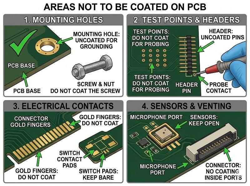
Nachstehend sind die wichtigsten Bereiche aufgeführt, die nicht beschichtet werden:
Steckverbinder und Kontaktstifte
Alle Steckverbinder, Kantenfinger, Buchsen und Kontaktflächen müssen unbeschichtet bleiben. Anwendung von Konforme Beschichtung auf diesen Oberflächen können die elektrische Leitfähigkeit blockieren und ein ordnungsgemäßes Zusammenfügen mit Kabeln oder Modulen verhindern. Dies ist eine der kritischsten Anforderungen an die Maskierung PCB-Montage.
Prüfpunkte und Programmierschnittstellen
Testpads, Messpunkte und Programmierleisten sollten frei von Beschichtungen gehalten werden, um elektrische Tests, Fehlersuche und Firmware-Updates zu ermöglichen. Unter Prototypische PCB-Montage, Der Zugang zu diesen Punkten ist besonders wichtig für die Validierung und Fehlerbehebung.
Schalter und mechanische Komponenten
Tasten, Relais, Steckbrücken und andere bewegliche Teile sollten nicht beschichtet werden. Die Beschichtung kann die mechanische Funktion beeinträchtigen oder dazu führen, dass Komponenten verkleben, was die Funktionalität in SMT-Bestückung Produkte.
Wärmesenken und thermische Schnittstellen
Bereiche, die für die Wärmeableitung vorgesehen sind, wie z. B. Kühlkörper, Wärmeleitpads oder Leistungskomponenten, sollten in der Regel unbeschichtet bleiben oder mit speziellen thermischen Beschichtungen versehen werden. Standardbeschichtungen können als Wärmeisolatoren wirken und die Wärmeübertragungseffizienz verringern.
Freiräume für Hochspannung
Bestimmte Hochspannungsbereiche können aus Sicherheits- und Leistungsgründen kontrollierte Abstände erfordern. Eine Beschichtung kann zwar die Isolierung verbessern, aber bei unsachgemäßer Anwendung können Lücken überbrückt oder Verunreinigungen eingeschlossen werden, was die Zuverlässigkeit beeinträchtigt. Eine sorgfältige Planung ist erforderlich bei PCB-Montage.
Erdungspunkte und Abschirmungsbereiche
Metallische Abschirmzonen oder Erdungskontakte sollten freiliegen, um eine ordnungsgemäße elektromagnetische Abschirmung und Erdung zu gewährleisten.
Steckverbinder für Hochfrequenzsignale (RF-Bereiche)
In HF-Schaltungen kann die Beschichtung die Impedanz oder die Signaleigenschaften verändern. Empfindliche Bereiche wie Antennen oder HF-Anschlüsse müssen unter Umständen unbeschichtet bleiben oder erfordern spezielle Materialien.
Optische Komponenten (LEDs, Sensoren)
LED-Linsen, optische Sensoren und Anzeigeelemente sollten nicht beschichtet werden, da die Beschichtung die Lichtübertragung blockieren oder verzerren kann. Unter SMT-Bestückung, Die Maskierung dieser Bereiche ist entscheidend für die Aufrechterhaltung der optischen Leistung.
Warum die richtige Maskierung wichtig ist
Werden diese Bereiche nicht geschützt, kann dies zu Problemen führen:
- Schlechte elektrische Verbindungen
- Schwierigkeit bei Prüfung und Reparatur
- Mechanisches Versagen von Komponenten
- Reduzierte thermische Leistung
Unter Prototypische PCB-Montage, In der Regel legen die Ingenieure die Maskierungszonen bereits in der Entwurfsphase fest und validieren sie durch Tests vor der Massenproduktion.
Bewährte Praktiken
- Eindeutige Kennzeichnung von Sperrzonen in Entwurfsdateien
- Verwendung von Abdeckbändern, Stiefeln oder Flüssigmasken
- Selektive Beschichtung für Präzision
- Durchführung einer Nachbeschichtungsinspektion zur Überprüfung der Sauberkeit
Zusammenfassend lässt sich sagen, dass nicht alle Bereiche einer Leiterplatte beschichtet werden sollten. Die ordnungsgemäße Identifizierung und der Schutz empfindlicher Zonen während PCB-Montage, SMT-Bestückung, und Prototypische PCB-Montage sicherstellen, dass Konforme Beschichtung erhöht die Zuverlässigkeit, ohne die Funktionalität zu beeinträchtigen.
Angebot für Conformal Coating einholen
Vom Prototyp bis zur Massenproduktion bieten wir konforme Beschichtungsdienstleistungen an. Fordern Sie jetzt Ihr Angebot an.
Senden Sie uns Ihre Anforderungen und erhalten Sie eine schnelle Antwort von unserem technischen Team.
✔ 24-Stunden-Reaktion ✔ Technische Unterstützung ✔ Klein- und Massenproduktion
Shenzhen Tengxinjie Electronics Co, Ltd.


