Nano 塗層 for PCB
Nano coating for PCB is an advanced type of 保形塗層 that uses nanotechnology to create an ultra-thin protective layer on the surface of electronic assemblies. It is designed to provide high-level protection while maintaining minimal thickness, making it ideal for modern miniaturized designs in PCB 組裝 和 SMT 組裝.
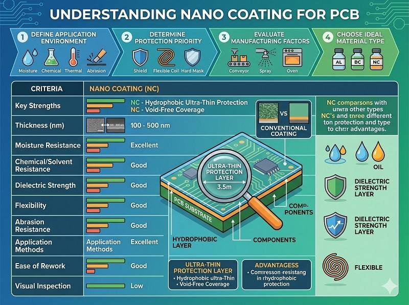
What is nano coating
Nano 保形塗層 is typically applied as a very thin film—often in the nanometer to micrometer range—compared to traditional coatings that are much thicker. Despite its thinness, it forms a highly effective barrier against environmental factors such as moisture, dust, and contaminants.
These coatings are often based on advanced materials like fluoropolymers or plasma-deposited films, which bond at a molecular level to the PCB surface.
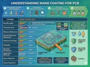
Key features of nano coating
Ultra-thin layer
Nano 保形塗層 is significantly thinner than traditional coatings, allowing it to protect circuits without adding bulk or affecting component spacing in high-density SMT 組裝.
Hydrophobic properties
Many nano coatings are water-repellent, preventing moisture from adhering to the PCB surface and reducing the risk of corrosion.
High transparency
The coating is usually transparent and does not interfere with inspection, testing, or optical components.
Minimal impact on weight and size
Because of its extremely thin structure, nano coating is ideal for compact and lightweight electronic devices.
Advantages in PCB 組裝 和 SMT 組裝
Nano 保形塗層 offers several benefits:
- Excellent protection against humidity and contamination
- Maintains electrical performance without altering design tolerances
- Suitable for compact, high-density PCB designs
- Allows easier rework compared to thicker coatings (in some cases)
Limitations to consider
Lower mechanical protection
Due to its thinness, nano coating provides less physical and abrasion resistance compared to thicker coatings like epoxy or polyurethane.
Limited chemical resistance
Some nano coatings may not perform as well in highly aggressive chemical environments.
Higher cost and specialized processes
Application methods such as plasma deposition or vapor-phase coating can increase manufacturing complexity and cost in PCB 組裝.
Typical applications
Nano 保形塗層 is commonly used in:
- Consumer electronics (smartphones, wearables)
- 醫療器材
- IoT and compact electronic modules
- High-density SMT 組裝 products
These applications benefit from protection without compromising size or performance.
總結
Nano coating is an innovative form of 保形塗層 that provides effective environmental protection with an ultra-thin layer. In PCB 組裝 和 SMT 組裝, it is especially valuable for compact and high-performance electronics where space, weight, and precision are critical. While it may not replace traditional coatings in all cases, it offers a modern solution for next-generation electronic protection.
取得保形塗層報價
Have special coating requirements? Send us your PCB files for evaluation.
Send us your requirements and get a fast response from our engineering team.
✔ 24-hour response ✔ Engineering support ✔ Small & Mass Production
深圳市騰欣杰電子有限公司