Coated on PCB
期間 保形塗層 於 PCB 組裝, 原型 PCB 組裝, 以及 SMT 組裝, it is essential to define keep-out areas—regions that must remain free of coating to ensure proper electrical performance, connectivity, and serviceability. Coating the wrong areas can lead to poor contact, signal issues, or even complete product failure.
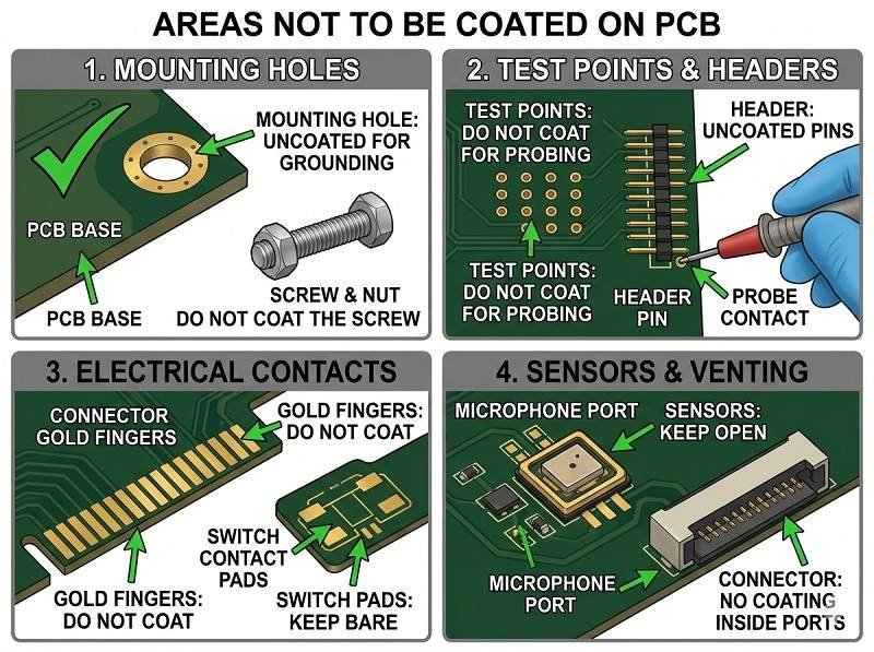
Below are the key areas that should not be coated:
Connectors and contact pins
All connectors, edge fingers, sockets, and contact pads must remain uncoated. Applying 保形塗層 on these surfaces can block electrical conductivity and prevent proper mating with cables or modules. This is one of the most critical masking requirements in PCB 組裝.
Test points and programming interfaces
Test pads, probe points, and programming headers should be kept free of coating to allow electrical testing, debugging, and firmware updates. In 原型 PCB 組裝, access to these points is especially important for validation and troubleshooting.
Switches and mechanical components
Buttons, relays, jumpers, and other moving parts should not be coated. Coating can interfere with mechanical operation or cause components to stick, reducing functionality in SMT 組裝 產品。.
Heat sinks and thermal interfaces
Areas designed for heat dissipation—such as heat sinks, thermal pads, or power components—should typically remain uncoated or use specialized thermal coatings. Standard coatings may act as thermal insulators, reducing heat transfer efficiency.
High-voltage clearance gaps
Certain high-voltage areas may require controlled spacing for safety and performance. While coating can improve insulation, improper application may bridge gaps or trap contaminants, affecting reliability. Careful design consideration is needed during PCB 組裝.
Grounding points and shielding areas
Metal shielding zones or grounding contacts should remain exposed to ensure proper electromagnetic shielding and grounding performance.
Connectors for high-frequency signals (RF areas)
In RF circuits, coating can alter impedance or signal characteristics. Sensitive areas such as antennas or RF connectors may need to remain uncoated or require specialized materials.
Optical components (LEDs, sensors)
LED lenses, optical sensors, and display elements should not be coated, as the coating can block or distort light transmission. In SMT 組裝, masking these areas is crucial for maintaining optical performance.
Why proper masking matters
Failing to protect these areas can lead to:
- Poor electrical connections
- Difficulty in testing and repair
- Mechanical failure of components
- Reduced thermal performance
在 原型 PCB 組裝, engineers typically define masking zones early in the design phase and validate them through testing before mass production.
Best practices
- Clearly mark keep-out zones in design files
- Use masking tapes, boots, or liquid masks
- Apply selective coating for precision
- Perform post-coating inspection to verify cleanliness
In conclusion, not all areas of a PCB should be coated. Proper identification and protection of sensitive zones during PCB 組裝, SMT 組裝, 以及 原型 PCB 組裝 ensure that 保形塗層 enhances reliability without compromising functionality.
取得保形塗層報價
從原型到大量生產,我們提供保形塗層服務。立即取得報價。.
將您的需求傳送給我們,並獲得我們工程團隊的快速回應。.
24 小時回應 ✔ 工程支援 ✔ 小型與大量生產
深圳市騰欣杰電子有限公司