In the world of electronics, PCBA (Printed Circuit Board Assembly) is the backbone of nearly every device—from smartphones and laptops to industrial sensors and medical equipment. Unlike a bare PCB (Printed Circuit Board), which is just a non-conductive board with copper traces, a PCBA includes all the soldered components (chips, resistors, capacitors, etc.) that make electronics function.
If you’re searching for “how PCBA is made,” “PCBA manufacturing steps,” or “key stages in PCBA production,” this guide breaks down the process into clear, actionable steps. We’ll also highlight quality control (QC) checks and industry best practices to help you understand what makes a reliable PCBA.

1. Pre-Manufacturing Preparation: Lay the Groundwork
Before physical production begins, careful planning ensures the PCBA meets design specs and avoids costly errors. This phase is critical for preventing rework later.
Key Tasks:
- PCB Design Review: Engineers use software like Altium Designer or KiCad to finalize the PCB layout, checking for:
- Proper spacing between copper traces (to avoid short circuits).
- Component placement (ensuring parts fit and are accessible for soldering).
- Compliance with industry standards (e.g., IPC-2221 for PCB design).
- Gerber File Generation: The design is converted into Gerber files—the universal format used by manufacturers to print PCB traces. Gerber files include details like trace width, hole sizes, and solder mask layers.
- Bill of Materials (BOM) Validation: A BOM lists all components (part numbers, quantities, suppliers) needed for the PCBA. Manufacturers cross-verify the BOM to ensure parts are in stock, compatible, and meet quality grades (e.g., industrial vs. consumer-grade).

2. Bare PCB Fabrication: Create the “Base” Board
The first physical step is manufacturing the bare PCB—the foundation for component assembly.
Step-by-Step Fabrication:
- Substrate Cutting: Start with a large sheet of FR-4 (the most common PCB substrate, made of fiberglass and epoxy resin). The sheet is cut into smaller, individual PCB sizes using CNC routers or laser cutters.
- Copper Cladding: Both sides of the substrate are coated with a thin layer of copper (typically 1oz–2oz thickness) via electroplating. This copper will become the conductive traces.
- Trace Printing (Photoengraving):
- A photosensitive film (resist) is applied to the copper layer.
- The Gerber file’s trace design is projected onto the film, “exposing” the areas that will remain copper.
- The unexposed resist is washed away, leaving only the desired trace pattern.
- Etching: The PCB is dipped in a chemical solution (e.g., ferric chloride) that removes the unprotected copper. Only the printed traces remain.
- Drilling Holes: CNC drills create holes (through-holes or vias) for component leads or to connect layers in multi-layer PCBs. Holes are then plated with copper to ensure conductivity between layers.
- Solder Mask Application: A green (or custom-colored) solder mask is screen-printed over the PCB. This non-conductive layer protects copper traces from oxidation, prevents short circuits, and highlights component pads.
- Silkscreen Printing: A white silkscreen layer adds text (part numbers, logos) and component outlines to guide assembly.

3. Component Sourcing & Inspection: Ensure Quality Parts
Even the best PCB design fails with low-quality components. This phase focuses on sourcing and verifying parts to avoid defects.
Critical Steps:
- Sourcing from Reputable Suppliers: Manufacturers partner with authorized distributors (e.g., Digi-Key, Mouser) to avoid counterfeit components—a major risk in electronics. Counterfeit parts often fail prematurely or cause safety hazards.
- Incoming Quality Control (IQC): Every batch of components is inspected for:
- Correct part number, value, and packaging (e.g., SMD vs. through-hole).
- Physical damage (bent leads, cracked casings).
- Electrical performance (using multimeters or component testers for resistors/capacitors).
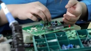
4. Component Placement: Precision is Key
Once parts are approved, they’re placed onto the bare PCB. Two methods are used, depending on component type:
A. Surface Mount Technology (SMT): For Miniature Components
SMT is the most common method for modern PCBs (used for 90%+ of components like chips, resistors, and LEDs). It’s faster and more precise than through-hole assembly.
- Solder Paste Application: A stencil (custom-cut to match component pads) is placed over the PCB. Solder paste (a mixture of tiny solder balls and flux) is squeegeed through the stencil onto the pads. The flux helps solder flow during heating.
- Pick-and-Place Machine: Automated robots (pick-and-place machines) use cameras to locate PCB pads. They “pick” components from reels/trays and place them precisely onto the solder paste-covered pads. Tolerances are as tight as ±0.1mm—critical for small components like 0402 resistors.
B. Through-Hole Technology (THT): For High-Power or Large Components
THT is used for components that need extra stability (e.g., connectors, transformers) or handle high current (e.g., power transistors).
- Manual or Automated Insertion: Component leads are inserted through pre-drilled holes in the PCB. Small batches may use manual insertion, while large-scale production uses automated insertion machines.
- Lead Trimming: Excess lead length is cut to 1–2mm above the PCB surface to prepare for soldering.
5. Soldering: Bond Components to the PCB
Soldering creates a permanent, conductive bond between components and PCB pads. The method depends on whether SMT or THT was used.
A. Reflow Soldering (for SMT Components)
- Reflow Oven Processing: The PCB (with placed SMT components) is sent through a reflow oven with controlled temperature zones:
- Preheat Zone: Gradually heats the PCB to 150–180°C to activate flux and evaporate moisture (prevents “popcorning” in chips).
- Soak Zone: Maintains temperature to ensure even heating across the board.
- Reflow Zone: Heats to 217–225°C (for lead-free solder) to melt the solder paste. The solder flows, bonding components to pads.
- Cooling Zone: Rapidly cools the PCB to solidify the solder, forming strong joints.
- Flux Cleaning (Optional): Some applications (e.g., medical devices) require cleaning residual flux with solvents to prevent corrosion.
B. Wave Soldering (for THT Components)
- Flux Application: The PCB’s bottom side (with THT leads) is sprayed with flux to remove oxidation.
- Wave Soldering Machine: The PCB is passed over a wave of molten solder (250–260°C). The solder adheres to the exposed leads and pads, creating a strong joint.
- Cooling: The PCB is cooled with fans to solidify the solder.
6. Post-Soldering Inspection & Testing: Catch Defects Early
No manufacturing process is perfect—inspection and testing ensure only functional PCBs move forward.
Common QC Checks:
- Visual Inspection:
- Manual checks (for small batches) or AOI (Automated Optical Inspection) (for large-scale production) use high-resolution cameras to detect defects like:
- Solder bridges (unwanted solder connecting two traces).
- Tombstoning (components standing upright due to uneven soldering).
- Missing components or incorrect placement.
- Manual checks (for small batches) or AOI (Automated Optical Inspection) (for large-scale production) use high-resolution cameras to detect defects like:
- Electrical Testing:
- ICT (In-Circuit Test): Uses a test fixture to check each component’s value, continuity, and connectivity. Ideal for catching short circuits or faulty parts.
- FCT (Functional Circuit Test): Powers the PCBA and tests its performance (e.g., a sensor PCBA would be checked for accurate data output). Ensures the PCBA works as intended in real-world use.
- X-Ray Inspection: For hidden defects (e.g., solder joints under BGA chips) that can’t be seen with AOI. Critical for high-reliability PCBs (aerospace, medical).
7. Rework (If Needed): Fix Defects Without Scrap
If defects are found (e.g., a solder bridge or faulty component), rework is performed to save the PCB:
- Desoldering: Tools like hot air stations or soldering irons remove faulty components or excess solder.
- Component Replacement: A new component is placed and resoldered.
- Re-Testing: The reworked PCBA undergoes inspection and testing again to confirm the defect is fixed.
8. Final Cleaning & Packaging: Prepare for Shipment
The last step ensures the PCBA is clean, protected, and ready for integration into the final product.
- Cleaning: Residual flux, dust, or debris is removed with ultrasonic cleaners or solvent-based cleaning systems (critical for PCBs used in harsh environments like automotive or industrial settings).
- Conformal Coating (Optional): A thin, protective layer (e.g., acrylic or silicone) is applied to the PCBA to shield it from moisture, dust, and vibration. Common in outdoor or high-humidity applications.
- Packaging: PCBs are packed in anti-static bags or trays to prevent electrostatic discharge (ESD)—a major risk that can damage sensitive components. Labels include part numbers, batch codes, and inspection dates for traceability.
Why Does the PCBA Manufacturing Process Matter?
A well-executed PCBA process ensures:
- Reliability: Fewer defects mean electronics last longer (e.g., a medical device PCBA must work without failure).
- Cost Efficiency: Early QC checks reduce rework and scrap, lowering production costs.
- Compliance: Following standards like IPC-A-610 (for PCBA acceptability) ensures PCBs meet industry and regulatory requirements (e.g., RoHS for lead-free manufacturing).