Ultra Small PCB Design
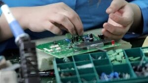
Ultra small PCB design This Bluetooth earphone circuit board features a highly integrated design, incorporating a low-power Bluetooth chip and an efficient audio processing module to ensure stable connectivity and clear sound quality. Precise PCB layout and high-quality components improve signal transmission efficiency while reducing electromagnetic interference, allowing the earphones to maintain excellent performance during exercise, commuting, or home use. Compared to ordinary circuit boards, it offers superior advantages in battery life optimization, heat management, and durability, making it a core component for creating high-quality wireless earphones.

Ultra-Small-PCB-Design: Challenges, Innovations, and Applications
Printed Circuit Boards (PCBs) are the backbone of modern electronics, providing the physical and electrical connections that allow components to function together. As devices become increasingly compact, the demand for ultra small PCB design has grown rapidly. This specialized field focuses on creating boards that are not only miniature in size but also capable of supporting complex functionality, high reliability, and efficient manufacturing. Designing ultra-small PCBs requires balancing electrical performance, mechanical constraints, and manufacturability, making it one of the most challenging areas in electronics engineering.
Miniaturization and Its Drivers
The push toward ultra-small PCBs is driven by several factors:
- Consumer electronics: Smartphones, wearables, and IoT devices demand compact boards to fit within sleek enclosures.
- Medical devices: Implantable sensors and portable diagnostic tools rely on miniaturized PCBs to reduce patient discomfort and improve usability.
- Industrial automation: Sensors and controllers often need to be embedded in tight spaces, requiring small yet robust PCBs.
These applications highlight the importance of reducing board size without compromising performance or reliability.

Key Design Challenges
Designing ultra-small PCBs introduces unique technical hurdles:
- Component density: With limited board area, components must be placed extremely close together, increasing the risk of interference and heat buildup.
- Signal integrity: High-speed signals on small boards are prone to crosstalk and electromagnetic interference, requiring careful routing and shielding.
- Thermal management: Smaller boards have less surface area for heat dissipation, making thermal design critical.
- Manufacturing tolerances: Ultra-small PCBs often involve fine-pitch components and microvias, which demand advanced fabrication techniques and strict quality control.
Innovations in Ultra-Small PCB Design
To overcome these challenges, engineers employ several innovative techniques:
- HDI (High-Density Interconnect): HDI technology uses microvias, blind vias, and buried vias to maximize routing density while minimizing board size.
- Flexible and rigid-flex PCBs: Flexible substrates allow boards to bend and fold, enabling compact designs in irregular spaces.
- Advanced materials: High-performance laminates with low dielectric constants improve signal integrity and reduce losses in miniature designs.
- 3D integration: Stacking multiple PCB layers or embedding components directly into substrates helps achieve ultra-compact layouts.
These innovations make it possible to design boards that are both small and powerful.
Applications of Ultra-Small PCBs
Ultra-small PCBs are found in a wide range of industries:
- Wearable technology: Smartwatches, fitness trackers, and AR glasses rely on miniature boards to integrate sensors, processors, and wireless modules.
- Medical implants: Pacemakers, hearing aids, and glucose monitors use ultra-small PCBs to deliver life-saving functionality in tiny packages.
- IoT devices: Smart sensors and home automation products often require compact boards to fit into everyday objects.
- Aerospace and defense: Miniaturized electronics reduce weight and space requirements, critical for satellites and unmanned systems.
These applications demonstrate the transformative impact of ultra-small PCB design on modern technology.
Best Practices for Designers
Engineers working on ultra-small PCBs must follow best practices to ensure success:
- Early collaboration with manufacturers: Engaging fabrication partners during the design phase helps align design choices with manufacturing capabilities.
- Simulation and modeling: Using advanced CAD tools to simulate signal integrity, thermal behavior, and mechanical stress reduces design risks.
- Design for testability: Even small boards must include provisions for testing and debugging, such as test pads or built-in self-test circuits.
- Iterative prototyping: Building and testing multiple prototypes allows designers to refine layouts and validate performance before mass production.

Future Outlook
As technology continues to evolve, ultra small PCB design will play an even greater role. Emerging trends such as system-in-package (SiP) integration, chiplet architectures, and nanomaterials promise to push miniaturization further while enhancing performance. The convergence of electronics with biotechnology, wearable computing, and smart environments will ensure that ultra-small PCBs remain at the forefront of innovation.