The Precision Journey of a Circuit Board: A Complete Analysis from Design to Finished Product
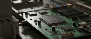
A printed circuit board (PCB) is the “neural network” of electronic devices, serving as the core carrier for electronic components and signal transmission. From smartphones and computers to aerospace equipment, almost all electronic products rely on it. Its production process integrates multiple techniques, including machining, chemical processing, and precision electronics. Each step requires strict control over precision and quality to ensure the stable operation of the final product.

I. Preliminary Design: Outlining the Circuit’s “Digital Blueprint”
The starting point of PCB production is circuit design, which directly determines the product’s functionality and performance. Engineers first use professional design software (such as Altium Designer and Cadence) to draw schematics based on the electronic device’s requirements, clarifying the connection relationships of components and signal paths. Subsequently, the schematic is converted into a PCB layout—planning the component layout, wiring paths, hole positions, and other key information on a virtual substrate, while considering factors such as electromagnetic compatibility, heat dissipation efficiency, and production feasibility. After the design is completed, it needs to be checked through DFM (Design for Manufacturing) to identify and eliminate potential production failures such as unreasonable layout, excessively thin wiring, and insufficient hole spacing. Once confirmed, the design files are exported in Gerber format (an industry-standard production file format) and transferred to the production workshop to officially begin the physical manufacturing process.

II. Substrate Preparation: Creating the “Physical Carrier” of the Circuit
The core substrate of the circuit board is usually a copper-clad laminate (CCL), which consists of an insulating layer (mostly epoxy resin fiberglass cloth, commonly known as “FR-4”) and conductive copper foil covering both sides. In the early stages of production, the CCL needs to be pre-treated according to design requirements:
- Cutting: Using a CNC cutting machine, large-size CCLs are cut to the required PCB board size, with an error controlled within ±0.1mm to ensure subsequent processing accuracy;
- Grinding: Mechanical grinding removes the oxide layer, oil, and impurities from the copper foil surface, increasing the adhesion between the copper foil and subsequent coatings;
- Cleaning and Drying: The board is rinsed with deionized water and then dried at high temperature to avoid residual moisture affecting the subsequent chemical treatment effect.
III. Circuit Fabrication: Etching Conductive “Signal Paths”
This is the most crucial step in circuit board production. Its purpose is to form the designed conductive lines on the copper foil. The main process involves “pattern transfer + chemical etching”:
- Coating with Photosensitive Ink: A layer of photosensitive ink (similar to photoresist) is evenly applied to the pre-treated copper-clad laminate surface. This ink cures under ultraviolet light.
- Exposure and Development: A film with the circuit pattern drawn is placed over the ink-coated board and exposed to ultraviolet light. The ink corresponding to the transparent areas of the film cures, while the ink in the opaque areas (i.e., the circuit areas) remains uncured. The board is then immersed in a developing solution, where the uncured ink is dissolved and removed, exposing the underlying copper foil.
- Chemical Etching: The developed board is immersed in an etching solution (commonly ferric chloride or copper chloride solutions). The copper foil not covered by ink is chemically etched away, leaving the desired conductive lines.
- De-inking and Cleaning: Finally, a de-inking solution removes the cured photosensitive ink from the circuit surface. After cleaning and drying, the circuit layer is fully formed. For multilayer circuit boards, after the single-layer circuit board is fabricated, a lamination process is used to bond the multilayer circuit board to the insulating layer. Simultaneously, a drilling and metallization process is used to achieve conductivity between layers.

IV. Hole Machining: Establishing “Connection Channels” Between Layers
Hole positions on circuit boards are mainly divided into two categories: “mounting holes” for mounting component pins and “vias” for conducting interlayer circuitry. The machining process is as follows:
- Drilling: According to the design documents, use a CNC drilling machine (drill bit diameter down to 0.1mm) to drill holes at the specified locations. The drilling accuracy must be controlled within ±0.05mm to avoid hole misalignment affecting component installation or signal transmission;
- Hole Wall Metallization: For vias in multilayer boards, a conductive copper layer is deposited on the hole wall using a “chemical copper plating + electroplating” process to achieve electrical connection between the upper and lower layers;
- Hole Finishing: Remove burrs and excess copper layer from the holes to ensure smooth hole walls and stable conductivity.

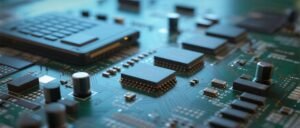
V. Solder Mask and Characters: Protecting Circuitry and Labeling Information
Solder Mask Fabrication: After the circuitry and hole machining are completed, a layer of photosensitive solder mask ink (usually green, but black, blue, etc. can also be used as needed) is applied to the surface of the board. After exposure and development, only the component lead soldering areas (pads) and some test points are exposed, while the rest of the circuitry area is covered by the solder mask ink. The purpose of the solder mask layer is to prevent circuit oxidation, avoid bridging and short circuits during soldering, and enhance the mechanical strength and environmental resistance of the circuit board.
Character Printing: Using screen printing or inkjet printing technology, component markings, polarity indicators, manufacturer information, and other characters (mostly white) are printed on the surface of the solder mask layer to facilitate subsequent component soldering and product repair.

VI. Surface Treatment: Enhancing Soldering Reliability
To prevent pad oxidation and improve wettability during soldering, surface treatment of the pads is necessary. Common processes include: Hot Air Leveling (HASL): Immersing the circuit board in molten tin-lead alloy (or lead-free tin alloy), then using hot air to level excess alloy on the pad surface, forming a uniform tin layer; Chemical Immersion Gold: Depositing a thin gold layer on the pad surface. Gold has good conductivity and oxidation resistance, suitable for high-precision, high-reliability products; OSP (Organic Solder Protectant): Forming an organic protective film on the pad surface. It is low-cost and suitable for circuit boards stored at room temperature and used for short periods.

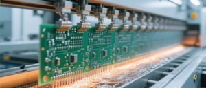
VII. Inspection and Packaging: Ensuring Quality and Delivery
After production, the circuit boards undergo multiple rigorous inspections to eliminate defective products:
- Electrical Performance Testing: Using a flying probe tester or in-circuit tester, the continuity and insulation of the circuitry are tested, and faults such as short circuits and open circuits are identified.
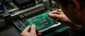
- Visual Inspection: Using manual visual inspection or AOI (Automated Optical Inspection) equipment, the circuitry is checked for etching defects, misaligned holes, peeling solder mask, and unclear characters.
- Reliability Testing: For high-requirement products, high and low temperature cycling, damp heat aging, and vibration tests are also conducted to verify their stability in extreme environments.
- Circuit boards that pass inspection are trimmed, deburred, and packaged according to specifications. They are typically sealed in anti-static bags with desiccants for moisture protection before being delivered to electronic equipment manufacturers for component soldering and assembly.