The Backbone of Modern Electronics -PCBA
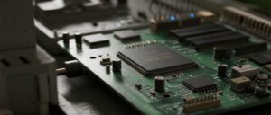
Printed Circuit Board Assembly (PCBA) is the unsung hero powering nearly every electronic device we rely on today. From smartphones and laptops to medical equipment and industrial machinery, PCBA serves as the critical interface that connects electronic components, enabling them to communicate and perform designated functions. Unlike a bare Printed Circuit Board (PCB)—which is merely a non-conductive substrate with copper traces—PCBA refers to the fully assembled board where components such as resistors, capacitors, integrated circuits (ICs), and connectors are soldered onto the PCB. This assembly process transforms a passive circuit board into an active, functional electronic module.

1. Core Components of a PCBA
The composition of a PCBA is a synergy of hardware and precision engineering, with each element playing a vital role in its performance:
- PCB Substrate: The foundation, typically made of FR-4 (glass-reinforced epoxy resin) for its durability, thermal resistance, and electrical insulation. High-performance applications may use materials like polyimide for flexibility or aluminum for better heat dissipation.
- Copper Traces: Etched copper layers forming intricate pathways that route electrical signals between components. The number of layers (single-sided, double-sided, or multi-layered) depends on the device’s complexity.
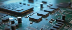
- Electronic Components:
- Surface-Mount Devices (SMDs): Miniaturized components attached directly to the PCB surface via solder paste, accounting for over 90% of modern PCBA components due to their compact size and high assembly efficiency.
- Through-Hole Components (THCs): Inserted through drilled holes and soldered on both sides, offering superior mechanical stability for high-stress applications (e.g., connectors, switches).
- Protective Layers: Solder masks (green/black coating) shield copper traces from corrosion and short circuits, while silkscreens print component labels, reference numbers, and brand logos for assembly and maintenance.

2. Key Stages in PCBA Manufacturing
PCBA production is a precision-driven process requiring advanced technology and strict quality control, consisting of six core stages:
- Design & Prototyping: Engineers use CAD software (e.g., Altium, Eagle) to design circuit layouts, optimizing component placement and trace routing to minimize signal interference. A prototype is then produced to test functionality.
- Bare PCB Fabrication: The designed layout is transferred to the substrate via etching, drilling (for through-holes and vias), and copper plating to enhance conductivity.
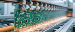
- Component Placement: Automated pick-and-place machines (capable of handling 10,000+ components per hour) place SMDs and THCs onto the PCB with micron-level accuracy, guided by computer vision systems.
- Soldering:
- Reflow Soldering: SMDs are bonded using solder paste melted in a convection oven (temperature controlled to 200–250°C).
- Wave Soldering: THCs are soldered by passing the PCB over a wave of molten solder (typically lead-free alloy).
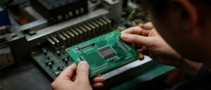
- Inspection & Testing:
- Automated Optical Inspection (AOI): Cameras detect soldering defects (e.g., bridging, missing components).
- Electrical Testing: Multimeters and oscilloscopes verify circuit continuity and signal integrity.
- X-Ray Inspection: Checks hidden solder joints (e.g., in BGA components).
- Cleaning & Final Assembly: Residues from soldering are removed, and the PCBA is integrated into the final device (e.g., housing, connectors).

3. Industry-Specific Applications of PCBA
PCBA’s versatility makes it indispensable across diverse sectors, each with unique requirements:
- Consumer Electronics: Compact, high-density PCBAs enable miniaturization in smartphones, wearables, and smart home devices. Flexible PCBAs (FPCBs) are used in foldable phones and laptops.
- Automotive: PCBAs power ADAS (lane departure warning, adaptive cruise control), EV battery management systems (BMS), and infotainment units. They must withstand vibration, extreme temperatures (-40°C to 125°C), and electromagnetic interference (EMI).
- Medical Devices: Ultra-reliable PCBAs are critical for pacemakers, MRI machines, and glucose monitors, requiring biocompatibility, low power consumption, and compliance with ISO 13485 standards.
- Industrial Automation: PCBAs in PLCs, sensors, and robotics ensure precise control and durability in harsh factory environments (dust, moisture, high voltage).
- Aerospace & Defense: Radiation-hardened PCBAs withstand extreme conditions (high altitude, temperature fluctuations) for satellites, aircraft navigation systems, and military equipment.

4. Emerging Trends Shaping PCBA Technology
As electronics evolve, PCBAs are adapting to meet new demands:
- Miniaturization & High Density: Driven by IoT and wearables, trends include microvias (diameter <0.15mm), blind/buried vias, and chip-scale packages (CSPs) to reduce board size while increasing component density.
- Green Electronics: Lead-free solders (e.g., Sn-Ag-Cu alloys) and eco-friendly substrates comply with RoHS and REACH regulations, reducing environmental impact.
- High-Speed & High-Frequency Performance: 5G, AI, and edge computing require PCBAs with improved signal integrity (controlled impedance traces) and thermal management (heat sinks, thermal vias) to handle faster data rates (up to 100Gbps).
- Flexible & Rigid-Flex PCBAs: These combine rigid and flexible layers, ideal for space-constrained or curved devices (e.g., wearable sensors, drone components).
- Additive Manufacturing: 3D-printed PCBAs are emerging, enabling rapid prototyping, custom shapes, and integration of conductive and non-conductive materials in a single process.
、盲孔_埋孔和芯.jpg)