Powłoka konformalna and potting
In electronics manufacturing, both Conformal Coating and potting are widely used to protect circuit boards during Montaż PCB oraz Montaż SMT. While they serve similar purposes—protecting electronics from environmental damage—their methods, materials, and applications are significantly different.
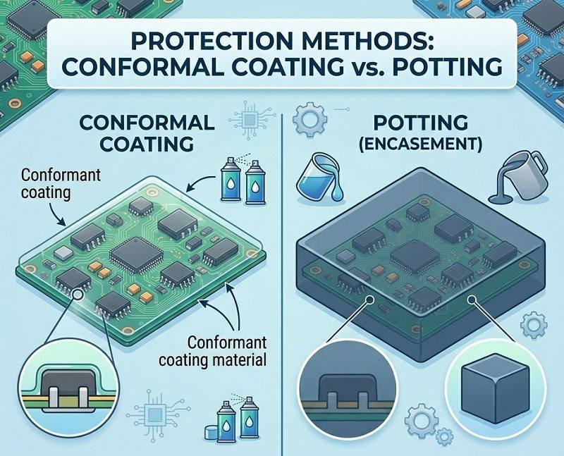
What is Powłoka konformalna
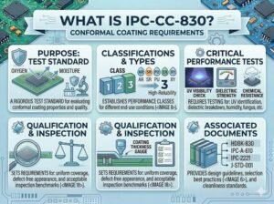
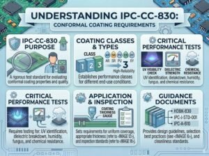
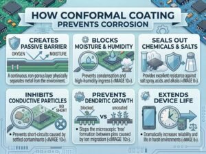
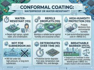
Powłoka konformalna is a thin, protective polymer layer applied directly to the surface of a printed circuit board. It “conforms” to the contours of components, creating a lightweight barrier against moisture, dust, chemicals, and temperature variations.
Because the layer is thin (typically 25–250 microns), it does not add significant weight or size to the board. This makes it ideal for compact and high-density designs in Montaż SMT. Additionally, coated boards can still be repaired or reworked if necessary, depending on the coating type.
What is Potting
Potting, also known as encapsulation, involves fully enclosing a PCB or electronic assembly in a solid or gel-like compound, such as epoxy, silicone, or polyurethane resin. Instead of a thin layer, the entire component or board is submerged and sealed within a protective material.
Potting provides a much thicker and more robust level of protection compared to Powłoka konformalna, making it suitable for extremely harsh environments. However, once potted, the electronics are usually impossible to repair or rework.
Key Differences
Protection Level
Potting offers superior protection against moisture, vibration, shock, and chemicals because the entire assembly is encapsulated. Powłoka konformalna provides effective protection but is designed for moderate environmental conditions.
Thickness and Weight
Powłoka konformalna is thin and lightweight, making it suitable for space-constrained designs. Potting adds significant bulk and weight, which may not be suitable for all applications.
Rework and Repair
Boards with Powłoka konformalna can often be repaired or modified. In contrast, potted assemblies are typically permanent, making rework nearly impossible.
Thermal Management
Powłoka konformalna allows better heat dissipation due to its thin layer. Potting can either help or hinder thermal performance depending on the material used, but it often traps heat if not properly designed.
Cost and Processing
Powłoka konformalna is generally more cost-effective and faster to apply during Montaż PCB. Potting involves more material and longer curing times, increasing overall production cost.
When to Choose Each Method
Powłoka konformalna is ideal for consumer electronics, telecommunications, and applications where size, weight, and serviceability matter. It is commonly used in Montaż SMT lines for efficient, scalable production.
Potting is better suited for harsh environments such as automotive, marine, military, or industrial equipment, where maximum protection is required and repair is not a priority.
Wnioski
Both Powłoka konformalna and potting are essential protection methods in Montaż PCB oraz Montaż SMT, but they serve different needs. Powłoka konformalna offers lightweight, flexible protection with the advantage of reworkability, while potting provides maximum durability and environmental resistance at the cost of size, weight, and serviceability. Choosing the right solution depends on your application requirements, operating environment, and budget.
Uzyskaj wycenę powłoki konformalnej
From SMT assembly to conformal coating, we offer one-stop solutions. Get a quote now.
Send us your requirements and get a fast response from our engineering team.
✔ 24-hour response ✔ Engineering support ✔ Small & Mass Production
Shenzhen Tengxinjie Electronics Co., Ltd.