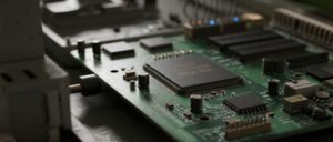
PCBA: The Core Hub of Electronic Devices
In the intricate construction of modern electronic products such as smartphones, smart home appliances, and industrial control equipment, the Printed Circuit Board Assembly (PCBA) plays a crucial role. It is not only the physical carrier of electronic components but also the core hub for realizing device functions. The PCBA organically combines electronic components with the printed circuit board (PCB) to form a complete circuit system, thereby driving the efficient operation of various electronic devices. Its mechanism of action encompasses multiple dimensions, including signal transmission, power distribution, and data processing, supporting a wide range of needs from everyday consumer electronics to high-end industrial equipment.

The Core Role of PCBA: The Cornerstone of Functional Realization
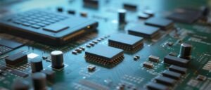
The core value of a PCBA lies in integrating discrete electronic components into a functional unit. This process begins in the circuit design phase, where engineers plan the circuit layout based on device requirements, determining component locations and connection paths. Subsequently, through surface mount technology (SMT) or through-hole mounting technology (THT), components such as resistors, capacitors, and integrated circuits are precisely soldered onto the PCB. This integration method not only optimizes space utilization but also significantly improves signal transmission efficiency. For example, in smartphones, PCBAs coordinate the collaborative work of components such as processors, memory, and sensors, ensuring smooth touch response, data processing, and wireless communication. Their functions can be summarized as follows:
Signal Transmission and Processing: As the “highway” for electronic signals, PCBAs enable rapid data exchange between components via copper foil traces, reducing signal delay and interference.
Power Distribution and Management: Integrating power management modules ensures stable voltage for different components, preventing equipment failures caused by power fluctuations.
System Integration and Optimization: Through compact layout, PCBAs support device miniaturization while enhancing heat dissipation and mechanical strength, adapting to complex environments.

Typical Application Scenarios of PCBAs: From Consumer Electronics to Industrial Control
PCBAs have extremely wide applications, and their design needs to be customized for different scenarios:
Consumer Electronics: In devices such as smartphones and tablets, PCBAs are responsible for integrating core functional modules, such as the connection between the processor and the display, and the control of the battery management system. For example, a high-efficiency PCBA can significantly improve device battery life and response speed, meeting users’ dual needs for portability and performance.
Industrial Control: Scenarios such as industrial robots and automated production lines place extremely high demands on the reliability and stability of PCBAs. They need to operate continuously under harsh conditions such as high temperatures and vibrations. Therefore, industrial-grade PCBAs typically employ ruggedized designs, such as adding protective coatings and redundant circuitry, to reduce failure rates.
Emerging Technology Fields: With the development of IoT and 5G technologies, PCBA applications in smart homes and wearable devices are increasing. These scenarios emphasize low power consumption and real-time data processing, driving the evolution of PCBAs towards greater precision and energy efficiency.

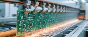
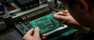
PCBA Design and Manufacturing: The Crystallization of Precision Technology
PCBA performance is highly dependent on design optimization and manufacturing processes. The design phase must consider signal integrity, electromagnetic compatibility (EMC), and thermal management, for example, reducing signal crosstalk through layered routing or using heat dissipation holes to improve component lifespan. The manufacturing process involves several key steps:
Component Placement: Using SMT technology, tiny components (such as chip resistors) are precisely placed onto PCB pads and fixed by reflow soldering. This step requires extremely high precision, with errors controlled within the micrometer level.
Soldering and Inspection: Wave soldering is used for through-hole components, and automated optical inspection (AOI) and X-ray inspection are used to ensure solder joint quality and avoid cold solder joints or short circuits.
Functional Testing: The assembled PCBA undergoes power-on testing to verify whether it meets design performance specifications, such as signal transmission rate and power consumption levels.
Future Trends of PCBA: Innovation-Driven Development
Faced with the increasingly complex demands of electronic devices, PCBA technology is undergoing rapid iteration. On the one hand, the application of high-density interconnects (HDI) and flexible printed circuit boards (FPC) allows PCBAs to adapt to more compact spaces and curved structures, such as foldable screen phones and wearable devices. On the other hand, environmental requirements are driving the use of lead-free soldering and recyclable materials to reduce the environmental impact of electronic waste. Furthermore, with the rise of artificial intelligence and edge computing, PCBAs need to integrate more intelligent functions, such as real-time data analysis and adaptive control, to support more complex application scenarios.

Conclusion: The Invisible Power of PCBAs
From the smooth operation of smartphones to the precise control of industrial robots, the importance of PCBAs as the “brain” and “neural network” of electronic devices is self-evident. Through precise design and manufacturing, it not only achieves efficient component collaboration but also drives continuous innovation in electronic technology. In the future, with breakthroughs in new materials and processes, PCBA will continue to play a crucial role in intelligentization, miniaturization, and green technology, bringing more possibilities to human life.