The Miniaturization Mandate
The trajectory of modern electronics is undeniable: devices must be smaller, lighter, faster, and more feature-rich. This relentless push for miniaturization and enhanced performance has put immense pressure on Printed Circuit Board (PCB) design and manufacturing. While traditional Through-Hole (TH) and standard Multilayer PCBs still serve many applications, the rise of complex, high-speed, and compact devices necessitates a paradigm shift to High-Density Interconnect (HDI) technology.
For design engineers and project managers, the question is not if HDI is superior, but when is the cost and complexity of HDI justified for their specific product? Adopting HDI is a critical engineering decision that impacts everything from board size and electrical performance to manufacturability and overall system cost.
This guide provides a comprehensive framework, rooted in four core decision-making criteria, to help you assess whether your next PCBA project has crossed the threshold into requiring HDI technology.
1. The Miniaturization Factor: When Space is the Primary Constraint
The most immediate and obvious driver for adopting HDI is space constraint. HDI technology allows for a dramatic increase in wiring density per unit area, often enabling a reduction in board size by 25% to 50% compared to a conventional design.
Key Indicators for Miniaturization:
A. High-Pin-Count, Fine-Pitch Components
The most common trigger for HDI is the adoption of advanced components, particularly Ball Grid Array (BGA) and Chip Scale Package (CSP) components with extremely small pitches.
- BGA Pitch Threshold: If your design features BGA packages with a pitch of 0.8mm or less (e.g., 0.6mm, 0.5mm, or 0.4mm), routing out the traces from the inner pin rows using standard through-hole vias becomes impossible or excessively complex.
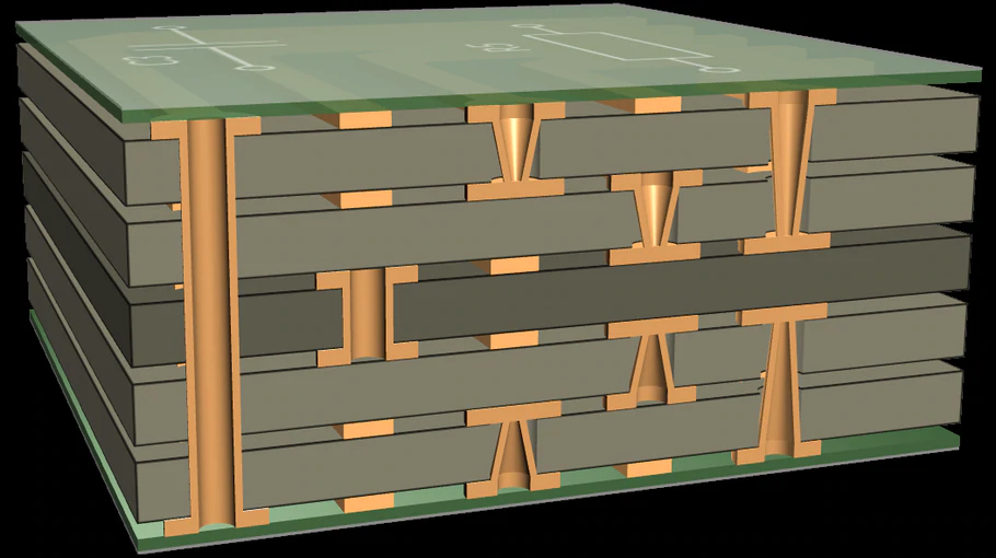
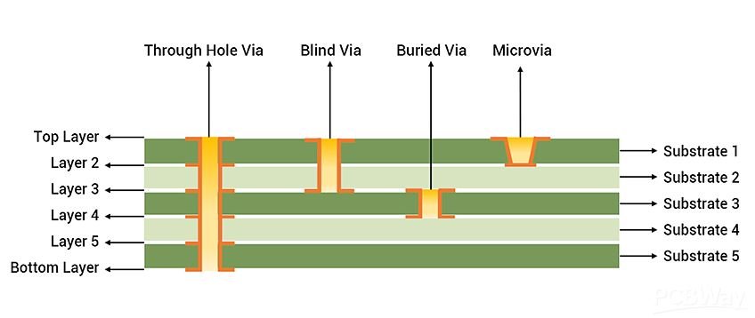
- HDI Solution: Via-in-Pad (VIP) and Microvias: HDI utilizes Microvias (laser-drilled holes typically less than 0.15mm in diameter) placed directly inside the component’s solder pad (Via-in-Pad). This technique frees up valuable surface area between the BGA pads for routing traces, drastically increasing density and allowing for the fan-out of high I/O count components in a smaller footprint.
B. Component Density and Layer Count Reduction
In traditional PCBs, high-density designs often force an increase in the total number of layers (e.g., from 8 to 12 layers) to accommodate all required traces. HDI can often achieve the same or greater routing complexity with fewer layers.
- The Layer-Count Paradox: An 8-layer standard PCB might be replaced by a 4-layer HDI board with two sequential build-up layers ($1+2+1$ or similar structure). This results in a thinner, lighter, and potentially lower-cost final board, despite the higher per-layer fabrication cost of HDI.
- Applications: This is non-negotiable for wearable devices (smartwatches, fitness trackers), smartphones, medical implants, and highly constrained aerospace electronics where every gram and cubic millimeter counts.
2. The Performance Factor: When Signal Integrity is Paramount
Beyond size, the primary electrical advantage of HDI lies in its ability to manage high-speed and high-frequency (RF) signals with superior integrity.
Key Indicators for Signal Integrity Needs:
A. High-Speed Interfaces and Data Rates
Modern interfaces like PCIe Gen 4/5, DDR4/5, USB 3.0/4.0, or 10G/40G Ethernet operate at frequencies where signal degradation due to long traces, reflections, and crosstalk is a major concern.
- Shorter Signal Paths: Microvias only span one or two layers (Blind or Buried Vias), unlike through-hole vias which traverse all layers and create an unwanted stub. This stub acts as a transmission line discontinuity, causing signal reflections (noise) at high frequencies. HDI’s microvias effectively eliminate the stub, drastically improving signal quality and enabling faster data transmission speeds.
- Tighter Impedance Control: The fine line widths and controlled dielectric thicknesses used in HDI construction facilitate more precise control over characteristic impedance (e.g., $50\Omega$ for RF or $100\Omega$ differential pairs for data), which is critical for minimizing signal loss and ensuring reliability.
B. Power Delivery Network (PDN) and EMI Management
High-speed processors and FPGAs require clean, stable power. HDI structures are inherently better for Power Delivery Networks (PDN).
- Decoupling Capacitor Placement: HDI allows for the placement of microvias directly in the pad of decoupling capacitors (Via-in-Pad). This minimizes the distance between the capacitor and the component’s power pin, reducing parasitic inductance and ensuring cleaner power delivery under high-current switching, thus lowering Electromagnetic Interference (EMI) across the board.
- Shielding: The ability to use stacked and staggered microvias allows for more robust and continuous ground planes, which are essential for effective EMI shielding in complex, multi-functional devices (e.g., a smartphone with Wi-Fi, 5G, GPS, and Bluetooth).
3. The Reliability Factor: When Durability and Longevity are Critical
In demanding environments—such as automotive, aerospace, or industrial controls—the PCB must withstand significant thermal and mechanical stress over its operational life.
Key Indicators for Enhanced Reliability:
A. High Thermal Cycling Stress
Components like those used in engine control units (ECUs) or outdoor communication systems are subject to wide temperature swings.
- Lower Aspect Ratio: Microvias in HDI boards have a significantly lower aspect ratio (the ratio of via depth to its diameter, often 1:1 or less) compared to traditional through-hole vias (which can be 8:1 or higher). A lower aspect ratio means the microvia barrels are far less prone to cracking or fatigue failure during thermal cycling (expansion and contraction of the board layers).
- Increased Structural Integrity: By replacing a large number of through-hole vias with smaller, more robust microvias, the mechanical integrity of the entire board is enhanced, leading to a longer product lifespan and fewer field failures.
B. Regulatory and Safety Compliance
For applications where failure is catastrophic (e.g., medical life support or aerospace flight controls), the enhanced reliability of HDI is a key compliance requirement. The ability to guarantee signal integrity and structural durability under stress makes HDI a preferred or mandated technology in these sectors.
4. The Manufacturing & Cost Factor: The Crossover Point
While HDI fabrication involves more complex processes (laser drilling, sequential lamination, copper filling), the overall system cost can often favor HDI at a certain complexity threshold.
Key Manufacturing Considerations:
A. The Crossover Point: When Complexity Simplifies Cost
The initial HDI manufacturing cost is higher due to advanced processes. However, a traditional PCB attempting to achieve the same density might require an impractical number of layers (e.g., 14, 16, or more) or an excessive board size.
- Cost Efficiency: Once the design complexity pushes the standard layer count beyond 8 or 10 layers, the cost savings from reducing the board size and the overall layer count using a $1+N+1$ or $2+N+2$ HDI structure often outweigh the increased per-layer fabrication cost. HDI consolidation can lead to savings in materials, assembly time, and enclosure costs.
- Design for Manufacturability (DFM): HDI’s use of Via-in-Pad technology actually simplifies assembly by providing clear, direct connections for BGAs, which can be critical for high-volume, automated SMT lines.
B. HDI Build-up Types (Sequential Lamination)
The type of HDI structure is defined by the complexity required:
- Type I ($1+N+1$): Single build-up layer on each side. Uses simple Blind Vias. (e.g., consumer laptops)
- Type II ($2+N+2$ Staggered): Two build-up layers on each side with Staggered Microvias. Higher density. (e.g., high-end graphic cards)
- Type III ($2+N+2$ Stacked): Two or more build-up layers with Stacked and Filled Microvias. Highest density, essential for routing ultra-fine pitch BGAs. (e.g., smartphones, servers).
The required BGA pitch and I/O count will dictate which HDI Type is necessary, directly influencing the manufacturing process and price.
Making the Right HDI Decision
The decision to transition to HDI technology should be driven by a cold, hard analysis of the product’s requirements against the four factors discussed: Space, Performance, Reliability, and Cost Crossover.
| Decision Criteria | Standard PCB (Recommendation) | HDI PCB (Requirement) |
| Miniaturization | BGA pitch $> 1.0 \text{mm}$; Low component density; No stringent size constraints. | BGA pitch $\leq 0.8 \text{mm}$ (especially $< 0.5 \text{mm}$); Wearables, handheld devices, medical implants. |
| Performance | Data rates $< 1 \text{Gbps}$; Non-critical impedance; Low-frequency applications. | High-speed interfaces (DDR4/5, PCIe Gen 4+); RF modules; Strict impedance and PDN control is needed. |
| Reliability | Controlled environment; Low thermal cycling. | Automotive, Aerospace, Industrial systems; High thermal or mechanical stress environment. |
| Cost Crossover | Layer count can be kept below 8; Standard via holes suffice for routing. | Standard layer count exceeds 10-12 layers to achieve routing; System size reduction outweighs NRE costs. |
As a PCBA quick production service provider, our role is to partner with you to analyze your Gerbers, BOM, and performance targets. By identifying the need for Microvias, Blind/Buried Vias, and advanced sequential lamination—the defining features of HDI—we ensure that your product’s performance and size goals are met with the most cost-effective and reliable manufacturing solution.
Do you have a specific BGA component or data rate requirement you would like us to analyze for an initial HDI feasibility assessment?