Common Problems and Solutions in PCBA Soldering Processes
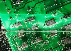
In the world of electronics manufacturing, the Printed Circuit Board Assembly (PCBA) process is the heartbeat of product reliability. However, as components shrink to microscopic sizes and board complexity increases, achieving a “perfect solder joint” every time is a significant challenge.
For European and American OEMs, quality isn’t just a metric—it’s a requirement for market entry. PCBA soldering defects can lead to costly recalls, field failures, and damaged brand reputations. Below, we explore the most frequent PCBA soldering issues and the engineering-grade solutions to mitigate them.

1. Solder Bridging
Solder bridging occurs when solder connects two or more adjacent pads or leads, creating an unintended electrical path (a short circuit).
The Root Causes
Stencil Design: Excessive solder paste deposition due to incorrect stencil thickness or aperture size.
Placement Accuracy: Misalignment of components during the Surface Mount Technology (SMT) pick-and-place phase.
Reflow Profile: A soak zone that is too short or a peak temperature that is reached too quickly.
The Solutions
Aperture Reduction: Reduce the stencil aperture size by 5–10% compared to the pad size to prevent paste overflow.
Advanced Inspection: Use Automated Optical Inspection (AOI) and Solder Paste Inspection (SPI) to catch bridging before the board ever enters the reflow oven.
Fine-Pitch Masking: Ensure a high-quality solder mask is applied between pads to act as a physical dam.

2. Tombstoning
Tombstoning is a common defect in small passive components (like 0201 or 0402 resistors/capacitors) where one end lifts off the pad, leaving the component standing vertically like a tombstone.
The Root Causes
Wetting Imbalance: One side of the component reaches the liquidus temperature before the other, creating a surface tension imbalance.
Uneven Heat Distribution: Large copper planes connected to one pad can act as a heat sink, slowing down the heating of that specific joint.
The Solutions
Thermal Relief: Use thermal relief traces for pads connected to large copper pours to ensure uniform heating.
Profile Optimization: Extend the “soak” time in the reflow profile to allow the entire board to reach a consistent temperature before the solder melts.
Nitrogen Environment: Using a nitrogen ($N_2$) reflow environment can improve wetting consistency across all pads.

3. Solder Balling
Solder balls are tiny spheres of solder that attach themselves to the solder mask or component bodies. While they might not cause an immediate short, they can dislodge later and cause intermittent failures.
The Root Causes
Moisture Contamination: Moisture in the solder paste expands rapidly during reflow, “popping” and scattering solder particles.
Excessive Pressure: Too much pressure during component placement can squeeze paste out of the pad area.
Oxidation: Using expired or improperly stored solder paste.
The Solutions
Strict Storage Protocols: Store solder paste in climate-controlled environments and allow it to reach room temperature naturally before opening to prevent condensation.
Pre-baking: For boards that have been exposed to humidity, a pre-bake cycle (e.g., 120°C for 4 hours) can remove trapped moisture.
Optimized Gasketing: Ensure the stencil makes a perfect seal (gasket) against the PCB during printing.

4. Voiding
Voids are “bubbles” or empty spaces within a solder joint. While small voids are often acceptable under IPC-A-610 standards, excessive voiding (usually >25% of the area) weakens the mechanical integrity and thermal conductivity of the joint.
The Root Causes
Outgassing: Volatile flux residues that don’t have enough time to escape before the solder solidifies.
Paste Quality: High levels of oxides in the paste.
The Solutions
Venting: Modify the stencil design to include “window pane” apertures for large thermal pads (like those on QFNs) to allow gas to escape.
Vacuum Reflow: For high-reliability sectors like aerospace or medical, using a vacuum reflow oven can pull gas bubbles out of the molten solder.
Flux Chemistry: Switch to a solder paste with a flux vehicle designed for low-voiding performance.
5. De-wetting and Non-wetting
Non-wetting occurs when the solder refuses to bond with the pad at all.
De-wetting occurs when the solder initially bonds but then pulls back, leaving a thin, grainy film.
The Root Causes
Surface Contamination: Oils, finger grease, or oxidation on the PCB pads or component leads.
Poor Plating: Low-quality PCB finishes (e.g., degraded HASL or thin ENIG).
The Solutions
Incoming Quality Control (IQC): Test the solderability of PCBs and components before they reach the production line.
Active Flux: Use a more active flux (if the design permits) to break through light oxidation layers.
Proper Handling: Enforce strict “no-touch” policies, requiring operators to wear gloves at all times.
Summary Table: Quick Troubleshooting Guide
| Problem | Primary Cause | Recommended Fix |
| Bridging | Stencil design / Alignment | Reduce aperture; improve SPI checks. |
| Tombstoning | Wetting imbalance | Add thermal relief; lengthen soak zone. |
| Solder Balling | Moisture / Expiry | Climate-controlled storage; pre-bake PCBs. |
| Voiding | Trapped flux gases | Use vacuum reflow; window pane stencils. |
| Non-wetting | Oxidation / Contamination | Improve IQC; use fresh flux/paste. |
Conclusion: The Path to Zero-Defect Manufacturing
In the competitive landscape of electronics manufacturing, the difference between a successful product launch and a failure often comes down to the details of the pcba soldering process. By implementing rigorous Dfm (Design for Manufacturing) reviews and maintaining a state-of-the-art SMT line, manufacturers can meet the exacting standards of Western clients.
Quality isn’t just about fixing problems—it’s about preventing them through data-driven process control and a culture of continuous improvement.