X-ray Inspection in PCB Assembly
Inspection par rayons X is an advanced, non-destructive testing method used in Assemblage du circuit imprimé to examine hidden solder joints and internal structures that cannot be seen with standard optical inspection. It plays a crucial role in modern Assemblage SMT, especially for complex components like BGA, QFN, and multilayer boards.
By using X-ray imaging, manufacturers can ensure the quality and reliability of solder connections inside the PCB without damaging the product.
Why X-ray Inspection is Needed
In many SMT components, solder joints are hidden underneath the package:
- BGA (Ball Grid Array) chips
- QFN (Quad Flat No-lead) packages
- LGA and other bottom-terminated components
Traditional AOI cannot inspect these areas, making X-ray inspection essential in high-reliability PCB Assembly.
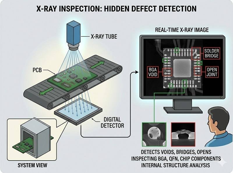
How X-ray Inspection Works
X-ray inspection systems operate by:
- Emitting X-rays through the PCB
- Capturing the transmitted radiation on a detector
- Creating an image based on material density differences
- Dense materials (like solder) appear darker
- Less dense areas appear lighter
This allows engineers to analyze internal solder joints and detect hidden defects.
What Defects Can X-ray Detect?
X-ray inspection is highly effective at identifying:
- Solder voids (air gaps inside joints)
- Bridging (short circuits between pads)
- Insufficient or excess solder
- Misaligned BGA balls
- Head-in-pillow defects
- Cracked or damaged solder joints
👉 These defects are often invisible in standard Assemblage SMT inspection methods.
Types of X-ray Inspection Systems
2D X-ray Inspection
- Produces flat images
- Faster and more cost-effective
- Suitable for general inspection
3D X-ray (CT – Computed Tomography)
- Creates 3D cross-sectional images
- Allows detailed internal analysis
- Ideal for complex PCB Assembly and failure analysis
Where X-ray Inspection is Used in PCB Assembly
X-ray inspection is typically performed:
- After reflow soldering
- During quality control and sampling
- In failure analysis and debugging
It is often used alongside AOI to provide complete inspection coverage.
Advantages of X-ray Inspection
- Non-destructive testing
- Ability to inspect hidden joints
- High accuracy for complex components
- Essential for BGA and fine-pitch devices
- Improves overall PCB Assembly quality
Limitations of X-ray Inspection
- Coût de l'équipement plus élevé
- Slower than AOI for large volumes
- Requires skilled operators for analysis
Despite these limitations, it is indispensable for advanced Assemblage SMT.
X-ray vs AOI Inspection
| Fonctionnalité | Inspection par rayons X | AOI Inspection |
|---|---|---|
| Visibility | Internal + hidden joints | Surface only |
| Vitesse | Modéré | Fast |
| Coût | Plus élevé | Plus bas |
| Application | BGA, QFN, complex boards | General SMT inspection |
👉 Both methods are complementary in PCB Assembly.
When Should You Use X-ray Inspection?
X-ray inspection is recommended when:
- Using BGA or bottom-mounted components
- Manufacturing high-reliability products (medical, automotive, aerospace)
- Performing failure analysis
- Ensuring strict quality standards
How to Optimize X-ray Inspection in SMT Assembly
- Use X-ray selectively for critical components
- Combine with AOI and SPI for full coverage
- Establish clear inspection criteria
- Train operators for accurate interpretation
Conclusion
X-ray inspection is a vital quality control technique in modern Assemblage du circuit imprimé et Assemblage SMT, enabling manufacturers to detect hidden defects that cannot be seen by optical methods. It ensures the reliability of complex electronic products and is especially important for advanced PCB designs.
By integrating X-ray inspection into the production process, manufacturers can significantly improve product quality and reduce the risk of failure in the field.
De la conception à la livraison, nous vous accompagnons à chaque étape. Demandez un devis pour l'assemblage de vos circuits imprimés.
Nous fournissons des services professionnels d'assemblage de circuits imprimés, y compris SMT, DIP et des solutions complètes clé en main.
✔ NDA disponible ✔ Devis rapide sous 24 heures ✔ Usine certifiée ISO ✔ Service unique de PCB et PCBA


