IResearch on the Basic Process Flow of Scanning Tunneling Microscopy (STM)
Abstract Scanning tunneling microscopy (STM) is an advanced instrument capable of imaging and manipulating material surfaces at the atomic scale. This paper systematically describes the basic process flow of STM, including sample preparation, probe preparation, tunneling measurement, data acquisition and analysis, and further explores its applications in materials science and nanotechnology. By outlining the process flow, this paper aims to provide researchers with a clear experimental operation framework.

1 Introduction
With the development of nanoscience, STM has become an important tool for studying the structure and electronic properties of solid surfaces. Its unique tunneling effect allows researchers to directly observe atomic arrangements and perform single-atom manipulation. To obtain high-quality experimental results, the STM process flow must strictly follow standardized procedures.

2 Sample Preparation
Surface Cleaning: Surface contaminants are removed using a combination of ion sputtering and high-temperature annealing.
Conductivity Requirements: Metal samples can be used directly; semiconductor samples require doping or surface modification to improve conductivity.
Fix and Position: Samples must be securely mounted on the sample stage and kept stable in an ultra-high vacuum environment.

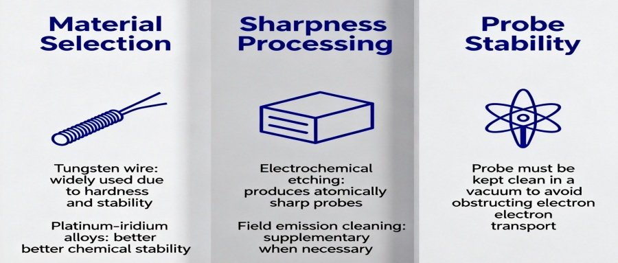
3 Probe Preparation
Material Selection: Tungsten wire is widely used due to its hardness and stability, while platinum-iridium alloys offer better chemical stability.
Sharpness Processing: Electrochemical etching can produce atomically sharp probes, supplemented by field emission cleaning when necessary.
Probe Stability: The probe must be kept clean in a vacuum to avoid obstructing electron transport.
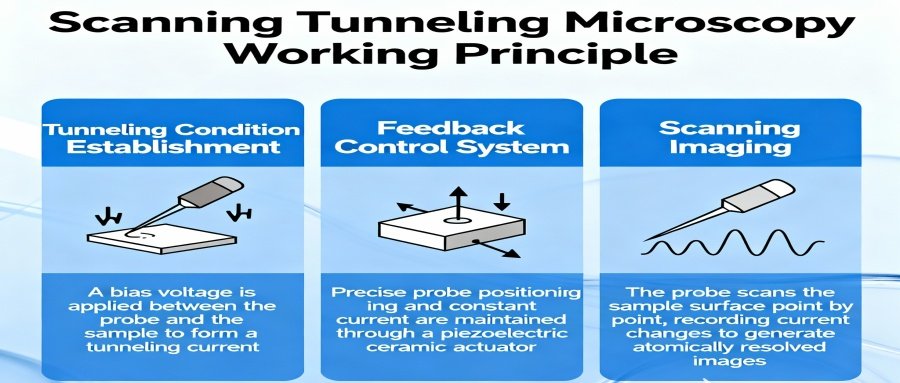
4 Tunneling Measurement
Tunneling Condition Establishment: A bias voltage is applied between the probe and the sample to form a tunneling current.
Feedback Control System: Precise probe positioning and constant current are maintained through a piezoelectric ceramic actuator.
Scanning Imaging: The probe scans the sample surface point by point, recording current changes to generate atomically resolved images.
5 Data Acquisition and Analysis
Image Reconstruction: Computer algorithms are used to convert the current signal into a three-dimensional surface topography map.
Spectroscopic Analysis (STS): By changing the bias voltage, local density of states information is obtained, revealing the electronic structure of the material.
Quantitative Research: Combined with theoretical models, in-depth analysis of defect distribution and surface reaction mechanisms is conducted.

6 Application Expansion
Surface Structure Research: Observing lattice defects, steps, and adsorbed atoms.
Nanofabrication: Manipulating individual atoms to construct nanodevices.
Materials Science: Studying the electronic properties of metals, semiconductors, and two-dimensional materials (such as graphene).
Quantum Device Exploration: STM demonstrates great potential in quantum dot and molecular electronics research.
Conclusion
The STM process encompasses key steps such as sample preparation, probe preparation, tunneling measurement, and data analysis. Its application in nanoscience and materials research not only promotes the development of basic science but also provides important technical support for future quantum devices and nanofabrication.