Coated on PCB
أثناء الطلاء المطابق في تجميع ثنائي الفينيل متعدد الكلور, تجميع النموذج الأولي لثنائي الفينيل متعدد الكلور, و تجميع SMT, it is essential to define keep-out areas—regions that must remain free of coating to ensure proper electrical performance, connectivity, and serviceability. Coating the wrong areas can lead to poor contact, signal issues, or even complete product failure.
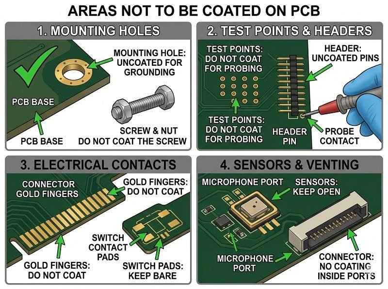
Below are the key areas that should not be coated:
Connectors and contact pins
All connectors, edge fingers, sockets, and contact pads must remain uncoated. Applying الطلاء المطابق on these surfaces can block electrical conductivity and prevent proper mating with cables or modules. This is one of the most critical masking requirements in تجميع ثنائي الفينيل متعدد الكلور.
Test points and programming interfaces
Test pads, probe points, and programming headers should be kept free of coating to allow electrical testing, debugging, and firmware updates. In تجميع النموذج الأولي لثنائي الفينيل متعدد الكلور, access to these points is especially important for validation and troubleshooting.
Switches and mechanical components
Buttons, relays, jumpers, and other moving parts should not be coated. Coating can interfere with mechanical operation or cause components to stick, reducing functionality in تجميع SMT المنتجات.
Heat sinks and thermal interfaces
Areas designed for heat dissipation—such as heat sinks, thermal pads, or power components—should typically remain uncoated or use specialized thermal coatings. Standard coatings may act as thermal insulators, reducing heat transfer efficiency.
High-voltage clearance gaps
Certain high-voltage areas may require controlled spacing for safety and performance. While coating can improve insulation, improper application may bridge gaps or trap contaminants, affecting reliability. Careful design consideration is needed during تجميع ثنائي الفينيل متعدد الكلور.
Grounding points and shielding areas
Metal shielding zones or grounding contacts should remain exposed to ensure proper electromagnetic shielding and grounding performance.
Connectors for high-frequency signals (RF areas)
In RF circuits, coating can alter impedance or signal characteristics. Sensitive areas such as antennas or RF connectors may need to remain uncoated or require specialized materials.
Optical components (LEDs, sensors)
LED lenses, optical sensors, and display elements should not be coated, as the coating can block or distort light transmission. In تجميع SMT, masking these areas is crucial for maintaining optical performance.
Why proper masking matters
Failing to protect these areas can lead to:
- Poor electrical connections
- Difficulty in testing and repair
- Mechanical failure of components
- Reduced thermal performance
في تجميع النموذج الأولي لثنائي الفينيل متعدد الكلور, engineers typically define masking zones early in the design phase and validate them through testing before mass production.
Best practices
- Clearly mark keep-out zones in design files
- Use masking tapes, boots, or liquid masks
- Apply selective coating for precision
- Perform post-coating inspection to verify cleanliness
In conclusion, not all areas of a PCB should be coated. Proper identification and protection of sensitive zones during تجميع ثنائي الفينيل متعدد الكلور, تجميع SMT, و تجميع النموذج الأولي لثنائي الفينيل متعدد الكلور ensure that الطلاء المطابق enhances reliability without compromising functionality.
احصل على عرض أسعار الطلاء المطابق
من النموذج الأولي إلى الإنتاج الضخم، نقدم خدمات الطلاء المطابق. احصل على عرض الأسعار الآن.
أرسل لنا متطلباتك واحصل على استجابة سريعة من فريقنا الهندسي.
✔ استجابة على مدار 24 ساعة ✔ دعم هندسي ✔ دعم هندسي ✔ إنتاج صغير وضخم
شركة Shenzhen Tengxinjie Electronics Co., Ltd.