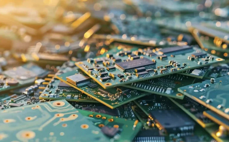
As modern electronic devices become more compact and powerful, Multi-layer PCBs have become an essential component in advanced circuit design. These boards integrate multiple conductive layers stacked together, allowing high-density connections, improved performance, and better reliability. This article explores the advantages, manufacturing principles, and applications of multi-layer PCBs, and how they differ from other PCB types.
What is a Multi-layer PCB
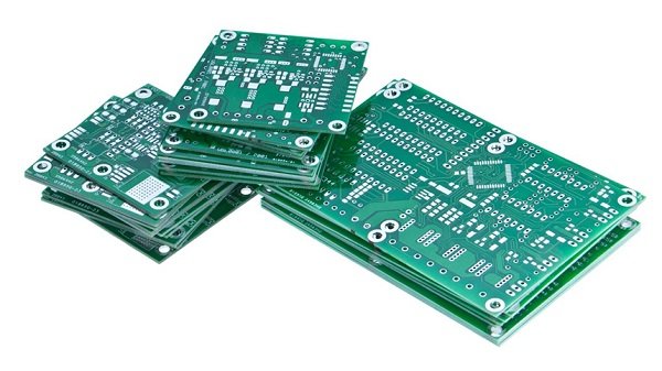
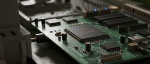
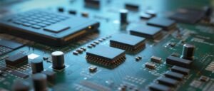
A Multi-layer PCB consists of three or more conductive copper layers separated by insulating materials and laminated together under high temperature and pressure. Unlike single or double-layer PCBs, multi-layer designs enable complex electronic circuits to be integrated into smaller spaces, offering high-speed performance and enhanced signal integrity.
Structure of Multi-layer PCB
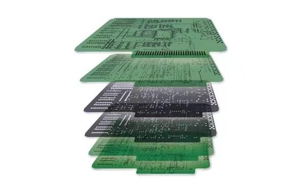
A typical multi-layer PCB includes alternating layers of copper and dielectric materials. The inner layers are used for signal routing, while outer layers support component mounting. Vias—through, blind, or buried—connect these layers electrically. This complex structure allows engineers to design compact yet powerful electronic boards.
Advantages of Multi-layer PCB
The advantages of multi-layer PCBs make them a preferred choice in modern electronics:
- High density and compact design – allows multiple circuits in limited space.
- Improved electrical performance – reduced crosstalk and signal loss.
- Better heat dissipation – due to the distributed copper layers.
- Enhanced durability – strong laminated structure offers stability.
- Increased functionality – supports high-speed and high-frequency applications.
Design Considerations for Multi-layer PCB
Designing a Multi-layer PCB requires careful planning of layer stack-up, trace routing, and via placement. Engineers must optimize:
- Power and ground plane distribution.
- Signal integrity and impedance control.
- Thermal management for high-power circuits.
- Material selection for mechanical and electrical stability.
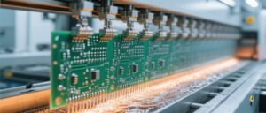
Manufacturing Process of Multi-layer PCB
The production of Multi-layer PCBs is more complex than that of single or double-sided boards. The main steps include:
- Inner layer imaging and etching.
- Layer alignment and lamination.
- Drilling and via plating.
- Outer layer etching and solder mask application.
- Final surface finishing and testing.
Each stage requires high precision to ensure perfect alignment and connectivity among layers.
Applications of Multi-layer PCB
Multi-layer PCBs are widely used in advanced electronic products that demand high performance and reliability, such as:
- Smartphones and tablets
- Telecommunication equipment
- Automotive control systems
- Medical devices
- Industrial automation
- Aerospace and defense electronics
Their compactness and performance make them ideal for space-limited and high-speed applications.
Multi-layer PCB vs Single-layer PCB
A single-layer PCB contains only one copper layer, making it cost-effective and simple to produce. However, it lacks the complexity needed for high-performance electronics. Multi-layer PCBs, by contrast, support complex circuitry, smaller form factors, and better electrical performance—at a higher cost but significantly greater functionality.
Multi-layer PCB vs Double-layer PCB
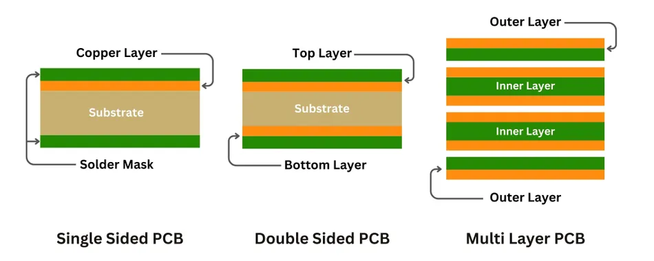
Double-layer PCBs feature two conductive layers, suitable for moderate-complexity circuits. However, multi-layer PCBs provide enhanced routing flexibility, improved electromagnetic compatibility, and better signal transmission—making them suitable for high-speed data and power applications.
Challenges in Multi-layer PCB Manufacturing
Despite their advantages, producing multi-layer PCBs requires precise process control. Common challenges include:
- Alignment of multiple layers.
- Controlling dielectric thickness.
- Maintaining signal integrity in high-speed designs.
- Cost management for small production runs.
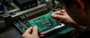
Why Choose Tenxinjie for Multi-layer PCB Solutions
At Tenxinjie, we specialize in PCB manufacturing and assembly for various industries. Our advanced facilities ensure accurate layer alignment, reliable soldering, and consistent quality for every Multi-layer PCB we produce. Whether you need prototype development or mass production, we deliver high-quality boards that meet your technical and budget requirements.