
In the world of electronic devices, the printed circuit board (PCB) is like the hidden brain that commands various components to work together in harmony. The quality of PCB layout design directly impacts the performance, stability, and reliability of electronic products. If you’re eager to delve into the mysteries of PCB layout design, this guide will open the door for you and lead you to master this crucial technology step by step.
The Importance of PCB Layout Design

PCB layout design isn’t just about randomly placing electronic components on the circuit board. A well-designed layout can reduce electromagnetic interference (EMI), improve signal integrity, minimize crosstalk, and ensure the stable operation of the circuit board under various environmental conditions. A good layout also boosts production efficiency and cuts costs as it reduces errors and rework during the manufacturing process.
Preparatory Work Before Design
Clarify Design Requirements
Before starting PCB layout design, it’s essential to clearly define the functional requirements, performance indicators, and usage environment of the electronic product. For example, if you’re designing a circuit board for high-speed data transmission, signal integrity will be a key factor; for battery-powered devices, power consumption and power management need to be given top priority.
Gather Component Information
Collect detailed information about all the electronic components to be used, including dimensions, pin definitions, and electrical characteristics. This information will help you determine the placement and connection methods of components on the circuit board. Also, understanding the package form of components is crucial, as different package forms can affect the compactness of the layout and the difficulty of wiring.
Select the Appropriate PCB Material
The choice of PCB material has a significant impact on the performance of the circuit board. Common PCB materials include FR-4 and metal substrates. FR-4 materials have good electrical and mechanical properties and are suitable for most ordinary electronic products; metal substrates offer better heat dissipation performance and are often used in high-power devices. Select the appropriate material according to the design requirements and understand its parameters such as thickness and number of layers.
Basic Principles of PCB Layout Design
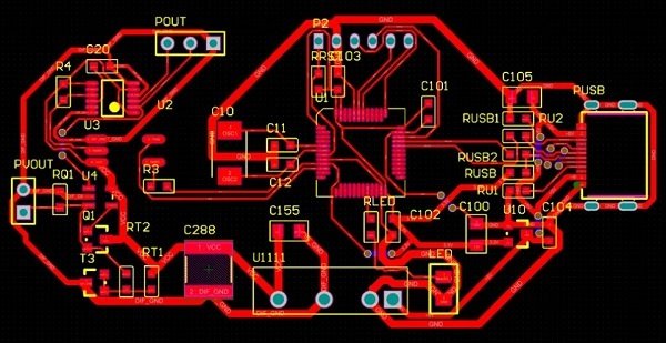
Component Placement
- Functional Zoning: Divide the circuit board into functional modules, such as power modules, signal processing modules, and interface modules. Place related components in the same area. This can minimize the signal path and reduce interference.
- Prioritize Core Components: First, determine the position of core components (such as microcontrollers and chip sets). Core components are usually at the center of the circuit board, and other components are arranged around them. Ensure there is enough space around core components for wiring and heat dissipation.
- High-Frequency Component Placement: High-frequency components should be placed as close as possible to reduce signal transmission distance, signal attenuation, and electromagnetic interference. Also, pay attention to separating high-frequency components from low-frequency components to avoid mutual interference.
- Heat Dissipation Considerations: For components that generate a large amount of heat (such as power devices), arrange a good heat dissipation path. Place them near the edge of the circuit board or in the heat dissipation channel, and use heat sinks or fans and other heat dissipation devices.
Wiring Rules
- Signal Integrity: To ensure signal integrity, minimize signal transmission delay and reflection during wiring. Avoid long traces, sharp corners, and branches. For high-speed signals, use appropriate wiring spacing and impedance matching.
- Power and Ground Lines: Power and ground lines should be made as thick as possible to reduce resistance and voltage drop. When using a multi-layer board, one layer can be dedicated to the power plane and another to the ground plane, which can improve power stability and anti-interference ability. Also, pay attention to power and ground segmentation to avoid interference between different power regions.
- Avoid Crosstalk: Maintain a certain distance between adjacent traces to avoid signal crosstalk. For sensitive signals (such as analog signals), you can use the method of grounding on both sides, that is, arrange ground lines on both sides to reduce external interference.
Electromagnetic Compatibility (EMC) Design
- Shielding Design: For components that are prone to generating electromagnetic interference (such as RF modules), use shielding enclosures. The shielding enclosure should be well grounded to ensure its effectiveness.
- Filter Circuits: Set up filter circuits at the power input and output terminals, signal interfaces, etc., to suppress the generation and propagation of high-frequency noise. Common filtering components include capacitors and inductors.
- Grounding Design: Good grounding is the key to EMC design. Adopt appropriate grounding methods such as single-point grounding, multi-point grounding, or a combination of both to ensure good grounding connections for all parts of the circuit board.
The Process of PCB Layout Design
Preliminary Planning
Create a new project in the PCB design software and set basic parameters such as the size, number of layers, and wiring rules of the circuit board. Roughly divide the areas of each functional module on the circuit board according to the principle of functional zoning.
Component Placement
Import the collected component libraries into the design software, and then place the components on the corresponding areas of the circuit board one by one according to their functions and layout principles. Pay attention to the direction and pin connection relationship of components during placement to ensure smooth wiring later.
Wiring
After completing component placement, start wiring. First, connect the power and ground lines to ensure the integrity of the power network. Then, connect the signal lines between components step by step according to the signal flow. During wiring, strictly follow wiring rules such as line width and spacing requirements. For complex circuit boards, you can combine automatic wiring and manual wiring to improve wiring efficiency and quality.
Design Inspection
After wiring is completed, conduct a comprehensive design inspection. The inspection content includes electrical rule checking (ERC), spacing checking, network connection checking, etc. Through these inspections, you can identify errors and violations in the wiring process and make timely corrections.
Optimization and Adjustment
Optimize and adjust the PCB layout according to the results of the design inspection and actual test conditions. For example, if you find that the electromagnetic interference in a certain area is large, you can adjust the position of components or add shielding measures; if there are problems with signal integrity, you can optimize the wiring length and impedance matching.
Common PCB Layout Design Mistakes and Solutions

Excessively Long Traces
Long traces can increase signal delay and electromagnetic interference. The solution is to readjust the position of components to shorten the signal path as much as possible.
Inadequate Wiring Spacing
Inadequate wiring spacing can easily lead to crosstalk and short circuits. Check the wiring spacing and adjust areas that do not meet the requirements to increase the spacing.
Power and Ground Issues
An unreasonable layout of power and ground can lead to unstable power supply and electromagnetic interference. Re-plan the power and ground wiring to ensure good grounding and power distribution.
Chaotic Component Placement
Chaotic component placement can affect the readability and maintainability of the circuit board. Rearrange the position of components according to the principles of functional zoning and layout to make the layout clearer and more reasonable.
Conclusion
PCB layout design is a task that requires patience and experience. By following the above principles and processes, as well as continuous learning and practice, you will be able to design high-quality PCB circuit boards. In the actual design process, fully consider the impact of various factors on the performance of the circuit board and flexibly apply various design techniques and methods. I hope this guide will be helpful to you on the path of PCB layout design and enable you to create even better electronic products.
If you are looking for professional PCB manufacturing and SMT patch services, welcome to choose TXJ. We provide one-stop solutions from design optimization to mass production to help your electronic project land successfully.