12 Fascinating Facts About PCB
PCB (Printed Circuit Boards) are the core component of nearly every electronic device, from smartphones to spacecraft. Though they may look like simple green or black boards, their design and manufacturing involve precision engineering. Today, we share 12 little-known facts about PCB to help engineers, buyers, and electronics enthusiasts better understand this critical technology.
PCBs Predate Computers
While modern PCB are inseparable from computers, their earliest concepts emerged in the 1920s. American inventor Charles Ducas first proposed printing conductive traces on insulated substrates in 1925—two decades before the first electronic computer, ENIAC (1946).
The Earliest PCBs Were Handmade on Breadboards

Before industrial PCB production, engineers manually connected circuits using “breadboards.” It wasn’t until the 1950s, when the U.S. military standardized PCB manufacturing, that they became mainstream in electronics.
Modern PCBs Can Have Traces Thinner Than a Human Hair
With advancements in microelectronics, high-end PCBs now feature trace widths as narrow as 3 micrometers (µm) —thinner than a human hair (~50–70µm). This precision is crucial for smartphones, chip packaging, and more.
Flexible PCBs Can Bend or Even Fold
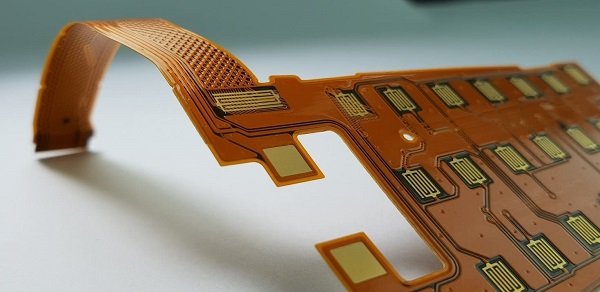
Flexible PCBs (FPCs) use materials like polyimide to bend, fold, or roll. They’re widely used in wearables (e.g., smartwatches), foldable phones, and medical devices.
Multilayer PCBs Can Exceed 100 Layers
Consumer electronics typically use 4–12-layer PCBs, but high-end servers, supercomputers, and aerospace PCBs can exceed 100 layers for ultra-high-density interconnects.
Color
Even if you know nothing about PCB, you must have a general appearance about it. PCB is usually viewed as green, which comes from the light transmitted from the solder mask glass painting. The solder mask is mainly used to protect the covered circuit from moisture and dust.
Why is the PCB solder mask green? For the earlier generation of military PCB, green, which was regarded as an army protection standard, was selected for protecting circuit reliability. Others take the opinion that the color of the epoxy resin used in the incipient solder mask painting is green, which is kept and used nowadays. As ages advance, green is not the exclusive choice. Multiple colors of solder masks are gain popularity as well.
Who invented the PCB

It’s well known that Bi Sheng, who lived in the Northern Song dynasty of China, invented printing. The earliest PCB, however, can go back to 1920, when the Austrian engineer Charles Ducas put forward the concept of conducting electricity through ink. Through electroplating technology, the wire can be directly made on the insulator surface, which is the prototype of the PCB.
Originally the metal wires on PCB were brass which is an alloy of copper and zinc. This great change not only eliminated the complex wiring procedure of electronic circuits but also ensured the reliability of circuit performance. However, it did not enter the practical application stage until the end of World War II.
Eco-Friendly PCBs Are a Growing Trend
EU RoHS regulations restrict hazardous substances (e.g., lead, cadmium), driving demand for halogen-free and recyclable PCBs. Green manufacturing is now an industry priority.
3D-Printed PCBs Are Revolutionizing Prototyping
Traditional PCB fabrication takes days or weeks, but 3D printing can produce prototypes in hours, drastically speeding up product development.
Electronic components
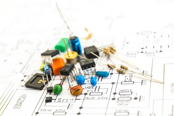
The function of the PCB is mainly accomplished by effectively connecting the components according to the schematic diagram. Each component plays its respective role, even the combination of every two parts that are closely adjacent on a PCB can also make a great difference. Basic components include resistors, diodes, transistors, PCB capacitors, batteries, transformers, etc.
Future PCBs May Integrate Biosensors
Researchers are developing PCBs with embedded biosensors to monitor heart rate, blood glucose, and more. Future medical devices could offer real-time health tracking.
China Is the Global Hub for PCB Manufacturing
China produces over 50% of the world’s PCBs, with major pcb manufacturing clusters in Guangdong and Jiangsu. Its mature supply chain offers significant cost advantages.
Conclusion
PCB technology continues to evolve, from high-density interconnects to flexible electronics and AI-driven design. The future promises even smarter and more efficient solutions. If you need high-quality PCB manufacturing or design support, contact us for expert solutions!

